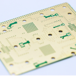
Solder Mask Opening: NSMD vs SMD Pad Design
A solder mask opening is the deliberate gap left in the protective coating so that copper can be exposed for soldering, probing or heat transfer. Everything else on the board stays covered, which is what stops the coating from interfering with the joint while it still protects the copper between joints. Getting the opening size and registration right is one of the quiet decisions that separates a board that assembles reliably from one that bridges at fine pitch.
What the Solder Mask Does
The mask is an insulating layer applied over the finished copper pattern and imaged with a photo tool, so it can be opened precisely where the design requires. It keeps the copper away from air and moisture, raises the surface insulation resistance between adjacent conductors, and prevents solder from wetting areas that are not meant to be joined.
Without it, every exposed conductor becomes a candidate for bridging during reflow, and the assembly would rely entirely on the accuracy of the paste deposit. That is why the mask and the openings are treated as a single design decision rather than as artwork decoration, and why mask quality is one of the first things checked when a new assembly shows an unexpected soldering defect.
Where Openings Are Needed
Component pads are the obvious case, and they include the surface mount lands, the through hole annular rings and the ball pads of a package array. Test points, fiducials and grounding pads also need to be open, because a probe or a screw has to reach bare metal rather than a film of coating.
Thermal pads are the case that is most often overlooked. A large exposed copper area under a power device helps spread heat into the board, but it also changes the amount of paste that is printed, and the opening is often subdivided into a window pane pattern to control solder volume and reduce voiding. Connector fingers and press fit zones are the remaining group, where the coating would add thickness that the mating part cannot tolerate.

NSMD and SMD Openings
The two conventions differ in which layer defines the pad. In a non solder mask defined pad, usually written NSMD, the opening is larger than the copper pad, so the mask never touches the land and solder wets the full copper surface. That gives a more uniform joint, spreads stress over the pad and is the usual choice for fine pitch packages.
In a solder mask defined pad, the opening is smaller than the copper, and the mask overlaps the edge of the land to anchor it and hold the pad size to the imaging tolerance rather than the etch tolerance. This is common for larger pads and for assemblies subject to mechanical load. Pad construction rules for both conventions are covered in pad design standards.
Expansion and the Solder Mask Dam
The opening is normally slightly larger than the copper it exposes, and the difference is called the expansion or clearance. A typical value is 3 to 4 mil on a standard board and 2 to 3 mil on an HDI build, with tight geometry designs going lower still when laser direct imaging is used. Too small an expansion leaves coating on the land and causes poor wetting; too large an expansion exposes adjacent copper and invites bridging.
The strip of mask left between two openings is the solder mask dam. It is the feature that keeps a fine pitch row of pads from bridging, and its width is limited by the imaging process: 4 mil is comfortable on a standard board, 2.5 to 3 mil is achievable on HDI, and 2 mil marks the practical edge of high end capability. A dam that is too narrow slumps or is washed away during development, and the defect becomes a bridge at the assembly stage.
Registration and Imaging
Mask registration is the alignment between the opening and the copper pad underneath it. Standard photo imaging holds roughly 3 mil, HDI holds about 2 mil and laser direct imaging holds around 1.5 mil. The number matters because the two errors, etch tolerance on the copper and imaging tolerance on the mask, add rather than cancel.
Where the mask is offset, one side of the pad is covered and the opposite side is over exposed. The covered side wets poorly and the exposed side has less dam, so the same board can show a cold joint on one pad and a bridge on its neighbour. That combination is a strong hint that the problem is registration rather than paste volume, and the ink behaviour that sets the limit is discussed in solder mask ink rheology.
Common Opening Defects
The failures cluster into a few groups. Offset openings follow exposure and material movement during imaging. Excessive copper exposure comes from an opening that is too large. Solder bridging appears at fine pitch where the dam is marginal, at QFN and package array pads, and where paste volume is high. Flaking or poor adhesion of the mask is a different problem, rooted in surface preparation or in the cure rather than in the artwork.
Two of these are worth separating because they look similar. A bridge caused by a missing dam comes back when the mask artwork is corrected; a bridge caused by excessive paste comes back when the stencil is corrected. Inspecting the board before assembly, under magnification, tells the two apart quickly and prevents a process change that fixes nothing.

Thermal and High Voltage Openings
Two applications push the opening design away from the standard rules. On a power device the exposed copper is a heat path, and a single large opening prints too much paste and traps voids under the part. Dividing the area into a grid of smaller openings, with mask crossing it in both directions, controls the paste volume and lets volatiles escape during reflow. Where the copper also connects to a via array, the vias are usually plugged and plated over before the mask is applied, as described in via in pad treatment.
On a high voltage board the opposite concern applies. Creepage and clearance distances must be maintained across the surface, and the mask is part of that insulation, so the opening is kept no larger than the joint requires and the coated gap between isolated regions is checked against the applicable standard. An opening that is generous for solderability can quietly reduce the surface distance below the requirement.
Controlling Quality in Production
Laser direct imaging writes the mask pattern without a film tool, which removes the dimensional error of the film and improves registration as well as allowing a narrower dam. Automatic optical inspection then checks the developed pattern for offset, opening size and missing or incomplete openings before the panel moves on, and electrical test confirms that no unintended connection has been exposed.
Standards control the outcome rather than the equipment. IPC-SM-840 covers the mask material itself, IPC-6012 covers the finished board, and IPC-A-600 defines what an acceptable opening looks like. A fabricator working to those documents will produce a repeatable result, and a specification that cites them avoids arguments about whether a given appearance is a defect.
FAQ
Should a fine pitch pad use NSMD or SMD? NSMD is the usual choice, because the larger opening lets solder wet the whole land and spreads the joint stress across the copper. SMD is reserved for pads that need the mask to anchor the copper or hold a tight pad size.
How much larger should the opening be than the pad? Roughly 3 to 4 mil on a standard board and 2 to 3 mil on HDI. The minimum usable value depends on the imaging process, and pushing below it risks coating left on the pad that prevents wetting.
Why do large thermal pads use a window pane pattern? To divide one large paste deposit into smaller areas, which reduces voiding during reflow and gives a more even solder layer under a power device while still exposing enough copper to carry heat away.