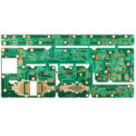
Solder Mask Registration And Opening Control
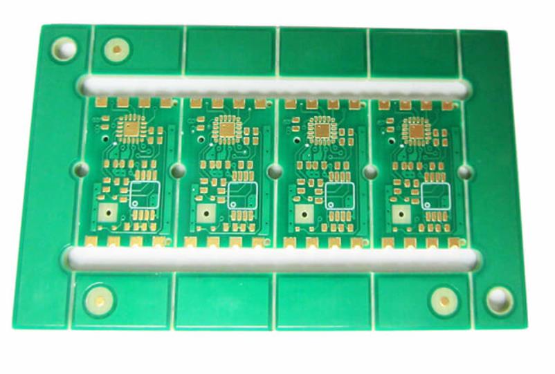
Soldermask registration is the alignment of the openings in the cured mask to the pads beneath them. It decides how much of each pad is exposed, how wide the mask dam between two pads remains, and whether the mask encroaches on a land that has to be soldered.
This article covers how the opening is defined, how the tolerance is built up, and what a misregistration does to the joint.
How The Opening Is Defined
The mask artwork defines an opening for every pad, and the opening is normally larger than the pad by a small amount on each side. The enlargement exists because the mask has to be clear of the pad edge, so that the solder can wet the whole land and so that the mask does not sit on the joint. The amount of the enlargement is one of the parameters a fabricator quotes as a capability, and it depends on the ink and on the process.
A larger opening exposes more of the copper and leaves more room for the mask to be misaligned; a smaller opening increases the risk that the mask encroaches on the pad and reduces the area available for the joint. The two effects set a practical range, and the choice within it depends on whether the design has a narrow dam to preserve. The ink behaviour that governs how the opening is formed is described under solder mask ink thixotropy.
Building Up The Tolerance
The opening position is subject to the imaging tolerance of the mask, the movement of the laminate during lamination and cure, and the registration of the mask to the copper pattern. The last of those is the largest term on a board with fine features, because the copper itself has an etch tolerance and the mask is aligned to the panel rather than to the individual pad.
The error is normally divided between the two sides of the opening, but the worst case is not the average. A pad at one edge of a panel may see the error in one direction and a pad at the other edge in the opposite direction, so the tolerance has to be applied in the worst direction for every pad rather than as a reduction in size. The pad geometry that absorbs that error is described under PCB pad design standards.
Effect On The Dam
The dam between two adjacent pads is the mask material left between their openings. Its width is the copper gap between the pads minus the enlargement on each side, and misregistration reduces it further on the side towards which the mask has moved. A dam that is reduced below the process minimum either fails to clear, leaving a veil of ink over the gap, or lifts at the edge during reflow.
Because the dam is the feature most sensitive to registration, the design rule for the opening is usually driven by the dam rather than by the pad. On a fine pitch footprint where the dam cannot be held at all, the pads are defined with a single opening that spans them, and the process then relies on the copper spacing to prevent bridging. The decision is made with the fabricator, because the capability is a property of the ink and the process rather than of the board.
Encroachment And Its Consequences
When the mask encroaches on a pad, the exposed copper is smaller than the design intended. The consequence depends on the direction and the amount. On the toe of a fine pitch lead, encroachment reduces the area available for the fillet and can leave a joint that looks thin. On a pad for a chip component, encroachment on one side shifts the effective centre of the land and can contribute to tombstoning, because the wetting force is no longer symmetric.
Encroachment also affects the deposit. The stencil aperture is positioned relative to the pad, and if the mask covers part of the pad, the paste is printed onto the mask rather than onto copper. The paste on the mask reflows into a ball instead of joining the joint, so a misregistration can produce balling rather than a visible mask defect. Both effects are reasons to keep the opening large enough that the worst case still clears the pad.
Measuring And Controlling Registration
Registration is measured optically on a sample, by comparing the position of the mask edge with the pad edge at several points across the panel. The measurement gives both the offset and the variation, and the variation across the panel is usually more important than the average, because a process that is centred but variable produces rejects at the extremes.
The controls are the imaging exposure and development, which set the opening size, and the lamination and cure conditions, which set the movement of the laminate. Curing the ink too quickly or at too high a temperature can move the opening, particularly on a thick film, and the cure profile is therefore part of the registration control rather than a separate step.
Design Rules And Coordination
The design rules should state the mask enlargement per side, the minimum dam width, and the minimum exposed pad dimension after the worst case registration. They should also state the fine pitch threshold beyond which the dam is removed and a single opening is used, so that the layout does not have to be reviewed pad by pad.
Because the capability depends on the fabricator, the rules should be agreed rather than assumed. A board transferred from one supplier to another with a tighter process may be built with a dam that the new supplier cannot hold, and the defect appears as intermittent bridging that is difficult to connect to the mask. Confirming the numbers before the artwork is released avoids that. The wider set of fabrication constraints is under design guidelines for manufacturability.
Additional Considerations for This Build
Practical attention to pad coverage pays for itself here, because it decides whether the finished board behaves as the drawing intended. Where the requirement is not stated on the fabrication drawing or in the assembly notes, the shop has to assume a default, and that default is rarely the value the design was simulated with. Stating pad coverage explicitly, together with the tolerance that applies, removes the assumption and keeps the result predictable from batch to batch.
Process Control and Verification
On a design of this kind, pad coverage is the item that decides how the rest of the board is arranged. Where a value sits close to a process limit, the drawing should say so, since the shop can then open the process window rather than working to a nominal figure that carries no tolerance. A stack-up that is drawn rather than described removes most of the ambiguity from a quotation, and it lets the fabricator price the board against the dielectric and copper weights that will actually be used.
FAQ
Why is the mask opening larger than the pad? So that the mask clears the pad edge in the worst case registration, leaving the whole land available for the joint. The enlargement is a process capability rather than a design preference.
Can a misregistration cause solder balls? It can, because paste printed onto the mask instead of the pad reflows into separate balls. The defect appears as balling rather than as a mask problem, which makes the cause easy to miss.
What is the minimum dam width? It comes from the fabricator, typically a few thousandths of an inch for a conventional ink, and it is narrower for a photoimageable mask. Below it, the dam is removed rather than made narrower.