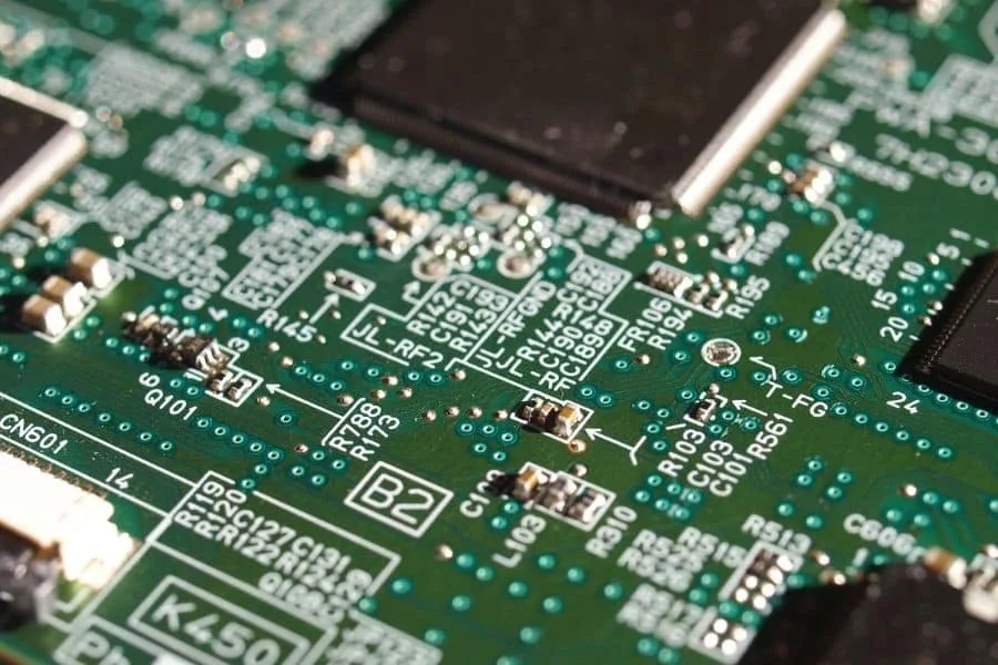
Solder Mask Thickness and Coverage Specification Guide
Solder mask is the thin polymer skin that decides where solder may flow and where copper must stay sealed. Designers often specify a colour and move on, yet solder mask thickness and coverage quietly influence yield, impedance, and long-term reliability. This guide walks through what the coating actually measures on a finished board, how standards classify coverage, and which process variables you must control to hit the specification every time.
What Solder Mask Thickness Really Means
The number quoted in a datasheet is rarely the number present on the board. Liquid mask is printed, dried, exposed, developed, and cured, so film thickness varies with copper height underneath. Over a bare laminate area the coating may measure 15 to 25 micrometres, while over a trace it can exceed 40. Buyers should therefore state where the measurement must be taken rather than assuming one figure describes the whole surface.
That variation is not a defect by itself. Mask thins over tall features because it flows away during levelling, and it thickens in open fields where nothing displaces it. The practical requirement is a minimum thickness above every conductive feature, held consistently across the panel. When a specification names a single value, it should also name the reference surface, the measurement method, and the sampling location.
Coverage Classes and Standards Requirements
IPC-6012, together with IPC-SM-840, describes mask coverage in qualitative classes rather than one universal number. Type T demands coverage over bare laminate only, Type H adds coverage across traces without covering the lands, and Type C requires the mask to cover everything except the areas intended for solder. Class 3 products for high-reliability use push that requirement further, with tighter visual and adhesion conditions.
Mass coverage matters as much as nominal thickness. Pinholes, skips, and thin patches that expose copper create sites for corrosion and electrochemical migration, especially near exposed rails or under humidity. A class 3 board therefore requires inspection for voids across the whole surface, not just at a few coupons. The mask coverage class you buy should match the environment the product will actually see.
How Thickness Is Measured on Real Boards
Cross-sectioning remains the reference method. A coupon is potted, ground, polished, and examined under a calibrated microscope, which reveals mask thickness over traces, laminate, and via walls at the same time. It is accurate but destructive and slow, so it is used for qualification and periodic auditing rather than routine screening. Sample locations must be chosen before the panel enters the lab.
Non-destructive alternatives include optical profilometry and eddy-current or ultrasonic gauges, which read film thickness without cutting the board. Each has limits: profilometry needs a clear area, gauges need calibration against a known sample, and none of them see under a component or inside a tented via. In practice, most fabricators combine a fast non-destructive check for trend monitoring with occasional microsections for proof.

Liquid Photoimageable Versus Dry Film Mask
Liquid photoimageable mask dominates rigid board production because it can be curtain-coated or screen-printed thin, images to fine resolution, and conforms to the copper topography. Dry film mask is a laminated sheet that offers very uniform thickness and excellent dielectric spacing, which suits some flexible circuits and thin boards, but it struggles to wrap over tall features and needs higher lamination pressure.
The choice affects the whole downstream process. Liquid cycles involve printing, pre-cure, exposure through a artwork, development, and a final thermal cure; dry film involves lamination, exposure, and development with no solvent flash step. Each route has its own thickness window, so a specification written for one chemistry cannot simply be copied onto the other.
Print Parameters: Mesh, Viscosity and Squeegee
When mask is screen-printed, mesh count, emulsion thickness, squeegee hardness, angle, and speed together set the wet deposit. A higher mesh count lays down less material and improves resolution, while a lower count deposits more thickness at the cost of definition. Viscosity drifts with temperature and solvent loss, so ink is usually held in a controlled window and stirred before use.
The press operator has the final influence. Too much snap-off distance or squeegee pressure pushes ink into openings, causing bridging between pads; too little leaves skips and thin fields. After printing, boards rest in a levelling zone so the ink flows out and solvent escapes evenly. Recording those parameters gives you a process that can be repeated rather than one that depends on a particular shift.
Solder Dam Width and Sliver Control
A solder dam is the narrow strip of mask that separates two adjacent pads and keeps molten solder from bridging them. Its width is limited by imaging resolution, so dams shrink with pitch: fine-pitch parts may call for the thinnest dams the process can hold while still surviving cure and assembly. Design rules usually specify a minimum dam width and a tolerance for slivers.
Slivers are thin mask filaments that break away, leaving loose particles on the surface. They form when artwork lines are narrower than the process can resolve consistently. A robust approach is to either widen the line to a manufacturable value or remove it entirely so the pads become one opening and are separated by the stencil instead. Decide this at design review, not on the shop floor.
Tenting and Via Coverage Decisions
Tenting means extending mask across a via opening so the barrel is covered on one or both sides. It protects the via from flux and solder, keeps contamination out of the hole, and prevents solder wicking away from a joint. However, a tent that is too thin or weakly adhered can crack during thermal cycling or outgassing, opening a path for moisture at exactly the wrong moment.
The alternative is to leave vias open, or to plug and plate them so the surface is flat. Tented vias are the cheapest option and work well on general-purpose boards, while via-in-pad and high-reliability designs usually prefer filled and capped structures. Whichever route you choose, the artwork, the fab notes, and the via drill data must all agree, or the fabricator will guess.

Cure, Adhesion and Thermal Cycling
Final cure converts the imaged film into a hard, chemically resistant coating. Under-cured mask stays soft, blisters during assembly, and releases ionic species; over-cured mask becomes brittle and cracks near pad edges. Manufacturers typically run a staged bake, sometimes with a UV bump, and verify the result with solvent rub, tape test, or differential scanning calorimetry on witness coupons.
Adhesion is tested after thermal stress because that is where the coating earns its keep. Boards pass through reflow at 245 to 260 degrees Celsius, then may be baked, wave soldered, or cycled in the field. A mask that peels at a pad edge exposes copper and invites corrosion. If delamination appears after the first reflow, the cure schedule or surface preparation, not the artwork, is usually the culprit.
Inspection, Defects and Process Control
Visual inspection under suitable lighting catches skips, foreign matter, and obvious pinholes; automated optical inspection can screen for exposed copper and slivers at production speed. Neither proves thickness. Pair them with scheduled cross-sections and an adhesion check so that the visual result has a measurable foundation. Photographs of good and rejected boards keep the criteria consistent between inspectors.
Process control starts with the ink lot and the environmental conditions in the print room. Temperature, humidity, and solvent content all shift viscosity, and a small change at printing becomes a large change after cure. Log the parameters you control, react to trends rather than single readings, and requalify whenever the supplier, colour, or chemistry changes. Mask is cheap; a field failure caused by a thin patch is not.
Related reading: our fabrication notes, board quality and design release notes cover the same ground.
FAQ
What is the typical solder mask thickness on a rigid PCB? Most specification calls are for 15 to 25 micrometres over bare laminate with a minimum of about 10 micrometres over any conductive feature. Values over traces run higher because the ink follows the copper. Always confirm the measuring surface and method with your fabricator, since a single blanket number cannot describe a topography that changes across the panel.
Should I tent vias or leave them open? Tent vias when you want to keep flux and solder out of the barrel and do not need to probe or wick them. Leave them open when the via must be tested, reworked, or used for thermal relief. For via-in-pad and fine-pitch BGA work, specify filled and capped vias instead, because a thin tent over a large opening can crack.
How do I know the mask is fully cured? Ask for the cure schedule and the evidence behind it, such as solvent rub results, tape adhesion after thermal stress, or calorimetry data. Visual gloss is not proof. If boards blister or peel after the first reflow, request a cross-section at pad edges and a review of the bake profile before assuming the laminate is at fault.