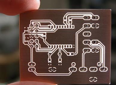
In modern electronic products, the printed circuit board is a fundamental part of almost every electronic system. The quality of the PCB directly affects the electrical performance, assembly yield, and long-term reliability of the finished product. For this reason, effective PCB Quality Control must begin well before the final assembly and functional testing stages.
In SMT Assembly, solder paste printing is one of the most critical processes because the quality of the printed solder paste directly determines the amount and position of solder available for subsequent reflow soldering.
If too much solder paste, too little solder paste, or no solder paste at all is deposited on a pad, the resulting solder joint may have insufficient mechanical strength or may create electrical defects after reflow.
Typical solder paste printing defects include:
- Insufficient solder paste
- Excessive solder paste
- Printing offset
- Solder bridging
- Missing solder paste
- Stencil aperture blockage
- Paste smearing
- Uneven paste deposition
- Inconsistent printing volume
Many of these defects can be identified before the PCB reaches downstream assembly processes through Solder Paste Inspection and inline machine-vision technologies.
Why Solder Paste Printing Quality Matters
Solder paste printing is often considered the first major quality-control point in the SMT process.
A typical SMT production flow includes:
PCB Loading → Solder Paste Printing → Solder Paste Inspection → Component Placement → Reflow Soldering → AOI/X-Ray Inspection → Electrical or Functional Testing
If a printing defect is not detected immediately, the PCB may continue through component placement and reflow.
At that point, identifying the original cause becomes more difficult and the cost of correction increases.
For example, an incorrectly printed pad may require:
- Component placement
- Reflow soldering
- AOI inspection
- Manual inspection
- Rework or component removal
If the defect is detected immediately after printing, the PCB may be corrected before additional manufacturing resources are consumed.
This makes Inline Inspection an important part of modern PCB Manufacturing.
Limitations of Downstream Inspection
Many PCB assembly lines use AOI, X-ray inspection, ICT, or functional testing to identify assembly defects.
These technologies are valuable, but they do not necessarily identify the original solder paste printing problem.
For example, an insufficient solder paste deposit may eventually result in:
- Open solder joints
- Weak solder joints
- Component displacement
- Non-wetting
- Intermittent electrical connections
A downstream inspection system may detect the final defect, but it may not clearly indicate whether the original problem occurred during printing.
This distinction is important for process improvement.
Solder Paste Inspection provides feedback much earlier in the manufacturing process, allowing operators and engineers to correct the printing process before the board moves to more expensive production stages.
What Is Solder Paste Inspection?
Solder Paste Inspection is an automated inspection process used to evaluate solder paste deposits immediately after printing.
Depending on the equipment, inspection may include:
- Solder paste area
- Paste height
- Paste volume
- X/Y position
- Shape
- Offset
- Bridging
- Missing paste
- Excessive paste
Modern SPI systems commonly use machine vision and, in many cases, three-dimensional measurement techniques to evaluate solder paste deposits.
Two-dimensional inspection can determine whether solder paste is present and whether its position and area are acceptable.
Three-dimensional inspection can additionally evaluate characteristics such as paste height and volume.
The inspection method should be selected according to the PCB design, package pitch, production requirements, and acceptable process variation.
Three Main Functions of Inline Vision Inspection
An integrated vision system within the solder paste printing process generally provides three major benefits.
1. Detect Defects Immediately After Printing
The first benefit is early defect detection.
The inspection system can compare the printed solder paste with the programmed reference conditions immediately after printing.
If the system detects excessive paste, insufficient paste, offset, bridging, or another abnormal condition, the operator can investigate the problem before the PCB proceeds through the rest of the SMT line.
This significantly reduces the risk of producing large quantities of defective assemblies.
2. Prevent Defects From Reaching Downstream Processes
Early detection prevents defective boards from moving into component placement and reflow.
This can reduce:
- Rework
- Scrap
- Component replacement
- Production downtime
- Root-cause investigation time
The earlier a defect is detected, the easier it generally is to isolate the relevant process parameter.
3. Provide Continuous Process Feedback
A good inspection system does more than simply classify individual boards as pass or fail.
It can provide process data that helps engineers identify trends.
For example, gradually decreasing solder paste volume may indicate:
- Stencil contamination
- Paste viscosity changes
- Printing pressure variation
- Squeegee wear
- Environmental changes
- Stencil aperture blockage
This makes inspection data useful for preventive process control.
PCB Pad Inspection
A vision system can inspect the solder paste deposited on individual PCB pads.
Typical inspection parameters include:
Printing Area
The system evaluates how much of the target pad area is covered by solder paste.
Insufficient coverage may lead to inadequate solder joints, while excessive coverage may increase the risk of solder bridging.
Printing Offset
The solder paste pattern is compared with the programmed pad position.
Excessive offset can cause uneven solder joints, particularly on fine-pitch components.
Solder Bridging
The system checks whether solder paste extends between adjacent pads.
If the distance between pads is small, excessive paste or poor printing alignment can result in bridging.
After reflow, this may become an electrical short circuit.
Paste Volume
For applications requiring tighter control, the system can evaluate solder paste volume.
Volume inspection is particularly useful for fine-pitch components and high-density assemblies where small variations in solder volume can affect joint quality.
Stencil Inspection
The stencil is another important part of the solder paste printing process.
A stencil contains apertures that determine where solder paste is transferred onto the PCB.
If an aperture becomes partially or completely blocked, the corresponding PCB pad may receive insufficient solder paste during the next printing cycle.
Therefore, Stencil Inspection can provide valuable information about stencil cleanliness and printing consistency.
Two common stencil-related defects are:
1. Aperture Blockage
Solder paste can remain inside stencil apertures after repeated printing cycles.
When an aperture becomes blocked, the amount of solder paste transferred to the corresponding PCB pad decreases.
This may result in insufficient solder volume.
2. Paste Smearing
Excess solder paste can accumulate on the stencil surface.
During subsequent printing, this material may spread to areas where solder paste should not be deposited.
Smearing can therefore contribute to:
- Printing contamination
- Poor pad definition
- Bridging
- Printing inconsistency
Automatic or operator-assisted stencil cleaning can help control these problems.
Camera Positioning and Image Acquisition
A conventional inline vision system uses cameras positioned above the PCB to capture images of the printed solder paste.
The inspection software then analyzes the captured image and compares it with programmed reference data.
The system can determine whether:
- Solder paste is present
- Paste is correctly positioned
- Paste coverage is within the programmed limits
- Adjacent pads are bridged
- Paste is missing
- The stencil requires cleaning
Accurate camera positioning is essential because the system must distinguish the solder paste from copper pads, solder mask, silkscreen, and other PCB features.
Lighting Is Critical for Vision Inspection
One of the challenges in machine-vision inspection is the variation in PCB surface reflectivity.
Different PCB surface finishes can produce different optical characteristics.
For example, HASL surfaces may have greater topographical variation than flatter surface finishes. Copper pads can also reflect light differently from solder mask or solder paste.
Therefore, lighting must be carefully designed to create sufficient contrast between the solder paste and surrounding PCB features.
The vision system may use different lighting angles or illumination techniques to improve image quality.
Good lighting helps the inspection algorithm identify:
- Pad boundaries
- Solder paste edges
- Printing offset
- Bridging
- Missing paste
- Surface contamination
Poor lighting can produce false positives or false negatives even when the vision algorithm itself is well designed.
Machine-Vision Software and Inspection Algorithms
Image acquisition is only the first step.
The inspection system must then process the captured images using appropriate algorithms.
Depending on the system, software may evaluate:
- Pattern matching
- Edge detection
- Area measurement
- Position offset
- Shape recognition
- Height
- Volume
- Statistical process trends
Reference data should be established based on the actual PCB design and manufacturing requirements.
It is important not to use excessively tight inspection limits simply to increase the number of detected abnormalities. Inspection thresholds should be correlated with actual assembly requirements and process capability.
Otherwise, excessive false alarms may reduce production efficiency without improving product quality.
2D and 3D Solder Paste Inspection
Solder paste inspection can generally be divided into two major approaches.
2D Inspection
Two-dimensional inspection evaluates the printed solder paste from the top view.
Typical measurements include:
- Presence/absence
- Area
- Position
- Shape
- Bridging
2D inspection can be fast and useful for many conventional applications.
However, it cannot directly measure the complete three-dimensional profile of the solder paste deposit.
3D Inspection
Three-dimensional inspection adds height information.
This allows the system to evaluate:
- Paste height
- Paste volume
- Area
- Position
- Shape
- Three-dimensional profile
3D Solder Paste Inspection is particularly useful for fine-pitch and high-density assemblies where solder volume and paste geometry are critical.
However, the required inspection capability should be selected according to the package technology, process window, and production requirements.
Solder Paste Inspection for Fine-Pitch Components
Fine-pitch components require tighter control of solder paste printing because the distance between adjacent pads is small.
Examples include:
- QFN
- QFP
- CSP
- BGA
- Fine-pitch connectors
- High-density IC packages
For these components, small printing offsets can significantly change the solder paste distribution.
Stencil design also becomes increasingly important.
Engineers may need to optimize:
- Aperture dimensions
- Aperture shape
- Stencil thickness
- Area ratio
- Pad-to-aperture relationship
- Solder paste selection
The optimal parameters depend on the component package and the specific PCB assembly process.
Factors Affecting Solder Paste Printing Quality
Inspection can detect defects, but stable production requires control of the factors that create those defects.
Stencil Condition
Stencil cleanliness and aperture condition directly affect paste transfer.
Solder Paste Properties
Important properties include:
- Viscosity
- Powder type
- Powder particle distribution
- Flux characteristics
- Storage condition
- Working time
Solder paste should be handled according to the material supplier’s specifications.
Printing Pressure
Squeegee pressure affects paste transfer.
Excessive pressure may produce inconsistent printing or increase paste spreading, while insufficient pressure may prevent proper stencil wiping.
Printing Speed
Printing speed influences paste roll behavior and transfer efficiency.
The optimum setting depends on the stencil, paste, PCB, and equipment.
PCB and Stencil Alignment
Accurate alignment is essential for fine-pitch assembly.
Even a small registration error can become significant when pad spacing is very small.
Environmental Conditions
Temperature and humidity can affect solder paste behavior and printing consistency.
Stable environmental conditions therefore contribute to more predictable SMT Assembly.
Closed-Loop Process Control
The greatest value of inline inspection comes when inspection data is used to control the process rather than simply record defects.
For example:
Printing → Inspection → Data Analysis → Process Adjustment → Reprinting
If the system identifies a gradual reduction in solder paste volume, engineers can investigate stencil cleanliness, paste condition, printing parameters, or equipment behavior before the problem creates a large quantity of defective boards.
This approach changes inspection from a purely reactive activity into a preventive manufacturing tool.
Common Solder Paste Printing Defects
The most common printing defects include:
Insufficient Paste
Possible causes include:
- Blocked stencil apertures
- Incorrect printing parameters
- Poor paste transfer
- Improper stencil design
- Paste condition problems
Excessive Paste
Possible causes include:
- Excessive paste deposition
- Poor stencil separation
- Excessive printing pressure
- Incorrect aperture design
Printing Offset
Possible causes include:
- PCB/stencil alignment errors
- Board movement
- Equipment calibration issues
- Poor fiducial recognition
Bridging
Possible causes include:
- Excessive solder paste
- Insufficient pad spacing
- Printing offset
- Poor stencil design
- Paste slumping
Missing Paste
Possible causes include:
- Blocked stencil aperture
- Printing failure
- Insufficient paste supply
- Incorrect programming
Integration With PCB Assembly Quality Control
Solder Paste Inspection should be considered part of a broader PCB Quality Control system.
A comprehensive SMT quality-control strategy may include:
SPI → Component Placement Verification → Reflow Profile Monitoring → AOI → X-Ray Inspection → ICT/Functional Testing
Each technology addresses different failure mechanisms.
For example:
- SPI focuses on solder paste deposition.
- AOI evaluates visible assembly features.
- X-ray can inspect hidden solder joints such as BGA connections.
- ICT evaluates electrical characteristics.
- Functional testing verifies system-level operation.
No single inspection technology can detect every possible defect.
The most effective approach is to use complementary inspection methods at appropriate process stages.
Benefits of Inline Inspection for PCB Manufacturers
For a PCB manufacturer or PCBA provider, inline inspection provides several important advantages.
Improved First-Pass Yield
Early detection reduces the number of boards that continue through the line with known defects.
Lower Rework Costs
Correcting a printing problem is generally simpler than repairing a finished assembly after reflow.
Better Process Traceability
Inspection data can be used to monitor trends and support process analysis.
Faster Root-Cause Analysis
When a defect is detected immediately after printing, engineers can focus on the printing process rather than investigating multiple downstream operations.
More Consistent Production
Continuous feedback allows process parameters to be adjusted before variations become major production problems.
Kingda’s Approach to PCB Quality Control
At Kingda, PCB Manufacturing and assembly quality are supported through process control at multiple production stages.
For SMT projects, solder paste printing can be evaluated according to the PCB design, component package, pad geometry, stencil structure, solder paste requirements, and assembly process.
Particular attention can be given to:
- Solder paste printing accuracy
- Stencil condition
- Fine-pitch components
- BGA and QFN assemblies
- Paste volume and position
- Printing consistency
- AOI and X-ray requirements
- Electrical testing
- Process traceability
- PCB Quality Control
By combining early-stage inspection with downstream assembly inspection, manufacturers can reduce process variation and improve overall production reliability.
Conclusion
Solder paste printing is one of the most important processes in modern SMT Assembly, and defects introduced at this stage can affect every subsequent manufacturing operation.
Solder Paste Inspection and Inline Inspection provide manufacturers with an effective method for identifying missing paste, insufficient paste, excessive paste, printing offset, bridging, stencil blockage, and other defects before they progress through the assembly line.
More importantly, inspection data can provide continuous feedback for process optimization.
For high-density PCB assemblies using BGA, QFN, CSP, and other fine-pitch components, accurate stencil design, solder paste control, printing parameters, machine vision, and process monitoring are particularly important.
A robust PCB Quality Control strategy therefore combines accurate solder paste printing, early defect detection, process feedback, and downstream inspection. By integrating these controls into PCB Manufacturing, Kingda helps customers achieve more stable assembly processes, higher production consistency, and reliable electronic products.