Solder Paste Mask Openings on Pads: What to Open and What to Close
The paste mask layer is the least examined layer in a finished design and one of the most consequential. It decides where the stencil will have an opening, and therefore where solder paste will be printed, and its defaults come from how a pad was created rather than from how the board will be built. Two boards with identical copper can assemble very differently if their paste mask layers differ, which is why the layer deserves a review of its own.
What the Layer Represents
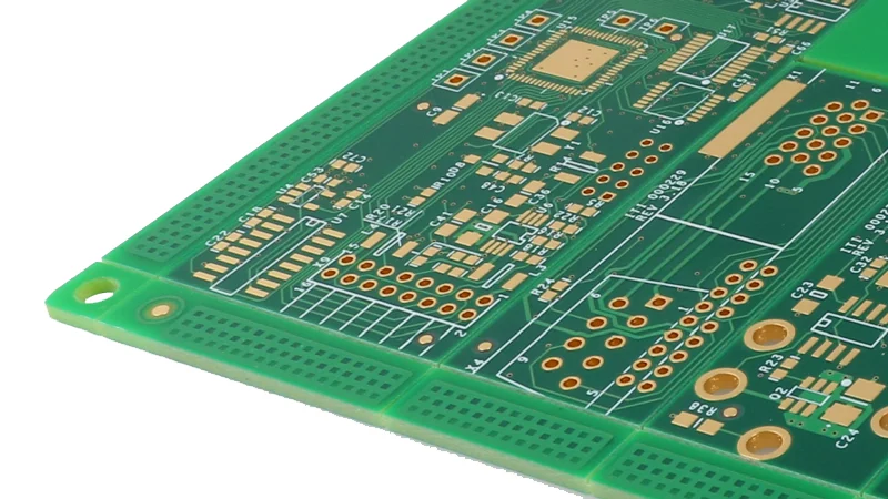
In the design data, the paste mask is a set of shapes that sit over the pads. What the fabricator does with them is separate: the paste mask information is passed to the stencil supplier, who cuts the openings into a stainless sheet, while the solder mask layer goes to the board shop to define the permanent coating. Confusing the two is the source of most of the errors in this area, because the solder mask opening and the stencil opening are decided by different people for different reasons.
The stencil aperture is what actually controls the deposit. Its area relative to the aperture walls determines how cleanly the paste releases, and its area relative to the pad determines how much solder ends up in the joint. Both of those relationships are geometry, and both of them are set by the paste mask shapes in the design file.
How the Defaults Are Derived
Most tools generate the paste mask automatically, and the rule they use is based on the pad type.
A pad that is defined on a single component side, which is the case for a surface mount pad, gets a paste opening by default. That is correct, because the part will be placed into a printed deposit.
A pad that is defined across all layers, which is what a plated through hole used for a through-hole part normally is, gets no paste opening by default. That is also correct for the common case, because a through-hole part is usually wave soldered or selectively soldered, and printing paste onto a hole would push solder into the barrel and create a mess.
The default follows the pad definition rather than the intention, and that is where it goes wrong. A through-hole pad that will in fact be pin-in-paste reflowed needs an opening that the default will not give it. A single-sided pad that carries a test point, a press-fit pin or a thermal pad that must stay free of solder needs no opening, and the default will give it one.

Closing a Pad Deliberately
Where a surface mount pad must remain free of solder, the paste opening is closed by making the paste shape smaller than the pad rather than by deleting the shape. Reducing the expansion value below the pad size, so that the paste shape is inset on all sides, produces an aperture that is too small for the paste to transfer through in any meaningful volume, and the pad is effectively closed while the design data stays complete.
The reason to keep a shape rather than to remove it is documentation. A pad that has no paste shape at all looks like an oversight in a review, whereas a pad with a deliberately inset shape is visible as a decision. It also survives library updates, since the pad still carries the information that it was considered.
The pads that most often need this treatment are the ones that would otherwise collect solder and cause a problem later. A test point with paste on it fills with solder and loses its flat surface. A pad that will carry a press-fit connector must stay clean, because the interference fit depends on the copper and the hole, not on a solder fillet. A thermal pad under a module that will be bonded with an adhesive rather than soldered must not be printed.
Opening a Through-Hole Pad
The opposite decision is needed for pin-in-paste. When a through-hole part is to be reflowed with the surface mount parts, the paste deposit has to supply the solder for the barrel and the fillet, and the volume required is much larger than the volume for a surface mount joint of the same pad size.
The standard approach is to open the paste mask over the through-hole pad and to modify both the aperture and the pad so that enough paste is available. The stencil is usually thinner for this reason, the aperture is enlarged beyond the annular ring, and the pad shape is often extended to create the extra printed area. The barrel itself is not printed; it fills by capillary action during reflow. If the volume is wrong, the joint is either starved or the solder balls on the surface next to the pad.
The parameters that make pin-in-paste work are the aperture area, the stencil thickness and the hole diameter, and they interact. A stencil that is thick enough to supply the volume for a large barrel may not release cleanly over the fine pitch parts elsewhere on the same board, which is why the process is normally reserved for boards where the mixed technology is the point of the design. Our mixed technology PCB assembly work covers both the printing parameters and the profile for these builds.
Paste Mask and Solder Mask Are Not the Same Shape
A second review point is the relationship between the two mask layers around a pad. The solder mask opening is normally larger than the pad, by an expansion value that the fabricator can manufacture reliably, so the pad is clear of coating on all sides. The paste opening on the same pad is normally the same size as the pad, or very slightly smaller.
The consequence is that the paste mask and the solder mask are not aligned by design, and if the paste shape is generated from the solder mask shape rather than from the pad, the aperture will be too large and every joint on the board will carry excess solder. Where a board is built with an unusually small solder mask expansion, the two shapes converge and the geometry has to be checked to make sure the aperture is still manufacturable.
The design rules that keep this consistent belong with the rest of the fabrication data, and they are reviewed with the stack-up rather than at the end of the layout. Our layout review covers the mask layers alongside the copper layers because a defect in either one produces a board that has to be scrapped.
How the Decision Reaches the Line
What the assembly partner receives is a stencil and a board, and the paste mask layer has already become a physical sheet. The visible consequences of a wrong decision appear at the other end: solder balls next to a filled test point, a press-fit pin that will not seat, a module that will not sit flat on its thermal pad.
Because the correction is expensive at that point, the check belongs earlier. A quick review of the paste mask layer against the assembly drawing, before the stencil is cut, catches every case in this article. Our SMT assembly team performs that review as part of the data package check, and our quality management records keep the stencil revision tied to the board revision so a later change cannot be printed with an old sheet.
FAQ
Should every surface mount pad have paste on it? No. Test points, press-fit pads, adhesive-bonded thermal pads and any pad that must stay clean should be closed deliberately.
Can paste be printed on a through-hole pad without changes elsewhere? Not successfully. Pin-in-paste needs a larger aperture, a different stencil thickness and often a modified pad to supply enough solder volume.
What happens if the paste shape is generated from the solder mask? The aperture becomes larger than the pad, more paste is deposited, and the joints carry excess solder that can bridge on fine pitch parts.