Bluetooth Speaker PCB Price: Board and Assembly Cost
A Bluetooth speaker hides a surprisingly dense board inside a small enclosure. Radio, audio amplifier, battery charger, power rails and user interface all share one substrate, and each block pushes the price in a different direction. This guide separates a Bluetooth speaker PCB price into bare board, components, assembly and test, shows where 2-layer and 4-layer designs diverge, and explains which cost adders are worth paying for in 2025.
What a Bluetooth Speaker Board Contains
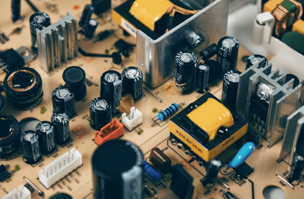
A Bluetooth speaker PCB carries four functional blocks: the radio module with its antenna, the audio path from converter to amplifier, the power subsystem with charger and battery management, and the user interface with buttons, LEDs or a touch controller. Miniature speakers usually integrate the radio and the control chip in one module, while larger products separate them to get better antenna placement.
That mix of analogue, digital and radio work on one board is what makes the design interesting. The radio needs a clean ground reference, the amplifier needs current and thermal headroom, and the charger needs creepage distance. Each requirement consumes area, and area is the first thing the fabricator prices, so the floor plan decides the cost long before the bill of materials does.
Bare Board Price by Design Class
Miniature portable speakers typically use a 2-layer FR-4 board with HASL finish, which lands in the low single-digit dollar range per piece in volume. Consumer models with a separate amplifier stage and a proper ground plane usually move to four layers. Outdoor and waterproof products add coating, a sealed enclosure interface and often thicker copper for thermal spreading.
Smart speakers with wake-word processing jump again. A microphone array, flash memory, a faster processor and sometimes Wi-Fi force a 4-layer or 6-layer board with controlled impedance traces. The bare board can cost several times the portable version, and the component count grows even faster than the board price itself.
Layer Count, Copper and Surface Finish
Layer count is the single largest lever on the bare board. Going from 2 to 4 layers adds two imaging steps, two lamination cycles and a plated core, which typically doubles the fabrication price before any assembly is considered. Whether that is justified depends on the radio: a well-laid-out 2-layer board with a solid bottom ground can pass EMC, but the margin is thin and the layout effort is higher.
Surface finish matters mostly for assembly yield. HASL is inexpensive and adequate for a board with small passives and a QFN amplifier. ENIG costs more but gives a flat surface for fine-pitch parts and a longer shelf life, which helps when boards are stored before a second assembly pass. OSP is the cheapest option but has a short shelf life and does not survive multiple reflows well.
Wireless Layout Requirements That Cost Money
Radio layout is where cheap boards get expensive. The antenna needs a keep-out area with no copper, no ground plane and no traces underneath, and the feed line needs a controlled-impedance feed line referenced to a continuous plane. If the module datasheet is followed loosely, the design can pass bench testing and fail certification, and a respin costs far more than the copper that was saved.
Shielding is the other cost. Amplifiers and switch-mode supplies radiate, and a metal can or a copper shield over the converter adds material, assembly time and a second reflow step. Designing the converter with a tight hot loop and a small input capacitor loop often removes the need for the shield entirely, which is the cheaper route when the layout is done well from the start.
Audio Path and Power Design
The audio path is analogue, and analogue design rewards area. A class-D amplifier needs a clean supply, short feedback loops and a filter placed close to the load. Its return currents should not share a path with the radio or the charger, so a sensible floor plan applies mixed-signal partitioning and joins the three blocks at a single reference point.
Power design follows the same logic. The battery charger, the boost converter for the amplifier rail and the low-dropout regulators for the processor all switch at different frequencies. Placing each converter next to the load it serves, keeping the inductor close to the switch node and using a local input capacitor keeps both noise and board area under control.
Assembly, Dispensing and Test Cost
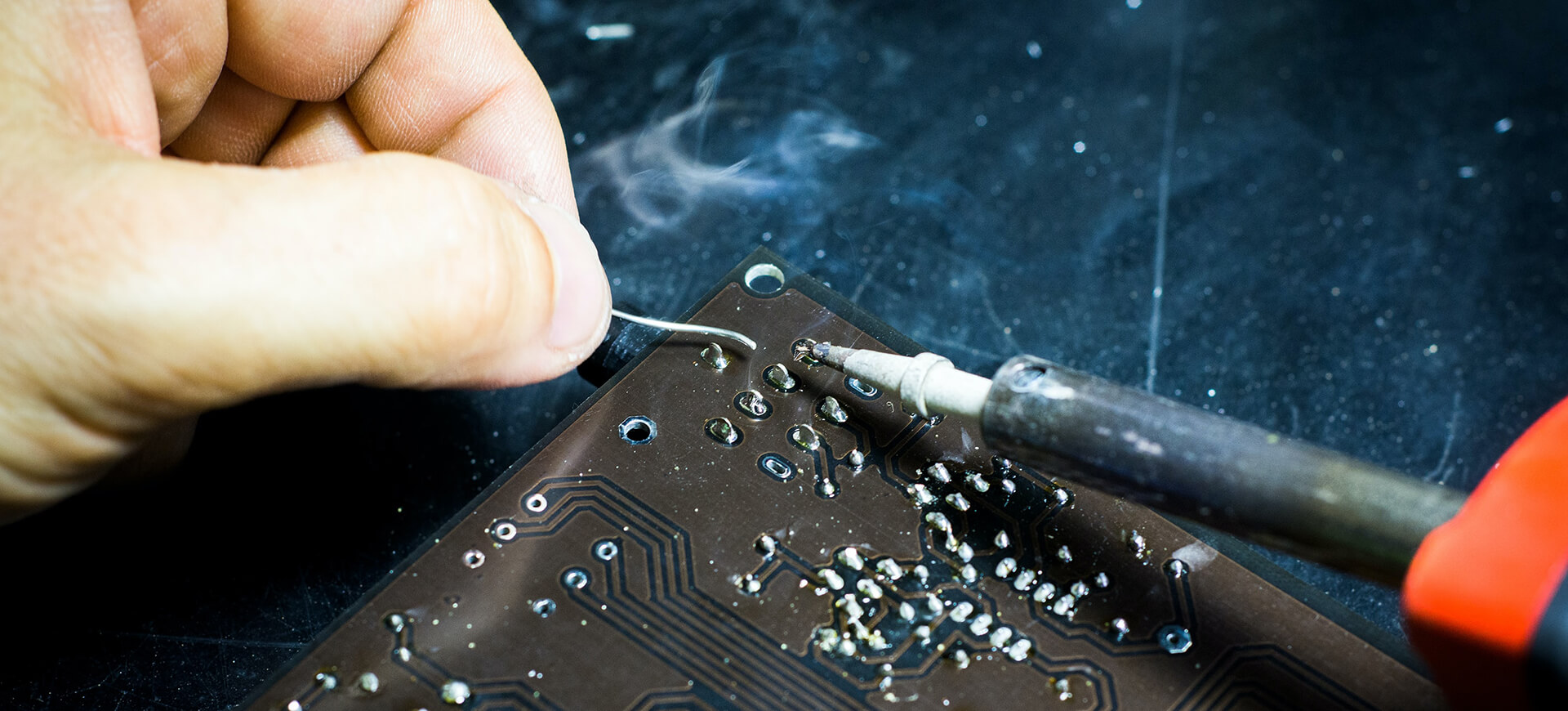
SMT assembly cost is driven by placement count and part mix, not by board area. A typical speaker board carries a few hundred placements, including a fine-pitch QFN amplifier that needs accurate paste deposition, sound pad geometry and placement order, and a well-controlled reflow profile. Double-sided assembly adds a second pass, a second stencil setup and a handling step that raises the risk of component shift during reflow.
Test adds the final layer. In-circuit test needs a fixture and test points; functional test needs a supply, an audio source and a measurement. For wireless products, radio functional test of transmit power and receiver sensitivity is normally the most expensive step per unit, because it needs shielded test equipment and a calibration routine that must be repeated for every unit.
Hidden and Indirect Costs
Indirect costs are easy to forget. Freight per board drops quickly with order size, duty depends on destination and declared value, and a small order carries an MOQ premium because setup time is spread over fewer units. Tooling for the stencil, the test fixture and the enclosure interface is billed once, but the amortised effect on a 500-piece order is significant.
Inventory and revision cost also matter. A single engineering change after the first build invalidates the test fixture, the stencil and often the board outline, so the total cost of a respin includes much more than the new boards. Freezing the design before tooling is ordered is the cheapest decision available, and it is usually the one that is postponed the longest.
Reducing Cost Without Hurting Sound Quality
The largest savings come from standardising. Using one 2-layer stackup across several speaker models, sharing a common module and reusing the charger circuit lets the fabricator run one set of tooling and a single stencil family. Standardising also shortens qualification, because the same board has already been through EMC testing once.
What should not be trimmed is the antenna keep-out, the reference plane under the radio feed, the supply decoupling around the amplifier and the thermal path under the converter. Each of those is a reliability feature rather than a luxury. Cutting them shows up later as certification failures, audible noise or field returns, all of which cost far more than the copper and area involved.
FAQ
Why does a 4-layer speaker board cost so much more than 2 layers? The extra layers add lamination cycles, imaging steps and a plated core, and they usually come with a finer minimum trace width. The bare board roughly doubles, and any controlled-impedance traces add a further charge because the fabricator must verify the stackup.
Can I use HASL on a board with a QFN amplifier? Yes. HASL is fine for 0.5 mm pitch packages as long as the paste volume and the stencil aperture are controlled. ENIG becomes worthwhile when the pitch is finer, when the board is stored for months, or when the assembly is double-sided.
How much does radio test add per unit? Radio functional test is the most expensive per-unit step because it requires shielded equipment and calibration. The per-unit cost falls with volume, but the fixture and the test programme are a fixed charge that should be budgeted before the first production build.