
Test Point Placement Rules for In Circuit Test Fixtures
Test points are the interface between a finished board and the machine that proves it works. Designers often scatter them at the end of layout, under whatever space is left, and the consequence is a fixture that costs more, probes less reliably and misses faults that should have been caught. Good test point placement is a design activity with rules that can be checked before release, and this article sets out those rules.
What Test Points Have to Deliver
A test point must present a stable, accessible surface to a spring loaded probe for the life of the fixture. That means enough copper area for the probe tip, a clean surface finish that does not oxidise, and mechanical support from the board beneath so the probe pressure does not flex the assembly.
It also has to be electrically meaningful. A test point on a net that is already accessible elsewhere adds nothing, while a missing point on a critical net forces the fixture to test the function indirectly or to skip it entirely.
Probe Geometry and Target Size
Probe geometry sets the minimum pad size. A typical fixture probe has a tip diameter between one and two millimetres, and the pad must be large enough that the tip lands inside the copper after accounting for placement tolerance and board movement in the fixture. A pad of 1.2 to 1.5 millimetres is a common working value for standard probes.
Smaller probes exist and allow tighter spacing, but they wear faster, need more precise fixtures and apply less force. Choosing them to save board area usually shifts cost into the fixture and into maintenance, so the decision should be made with the test engineer rather than by the layout alone.

Where the probe lands on a via rather than a dedicated pad, the via should be tented or left open deliberately, and its annular ring must be adequate for the tip.
Clearance Around Every Test Point
Each test point needs free space around it for the probe body, not just for the tip. A common rule is a keep-out of at least the probe diameter plus a margin, and taller components nearby must be excluded from the approach path since the probe travels vertically into the fixture.
Adjacent test points must be spaced so that neighbouring probes do not touch and so that a bent probe cannot short two nets. Spacing below about 1.5 millimetres should be treated as a special case that requires agreement with the fixture supplier.
Access on Both Sides of the Board
Fixtures can probe from the top, the bottom or both, and the choice affects cost and cycle time. Clam shell fixtures access both sides in one pass but are heavier and more expensive. Single sided fixtures are cheaper but require every test net to be reachable from one side.
Placement should follow the fixture strategy rather than the other way round. If the design intends a bottom side fixture, test points must not sit under tall top side components or inside a shield can that would obstruct the probe path.
Test Coverage and Net Selection
Coverage is the percentage of nets that the fixture can reach. Full coverage is not always necessary, but the nets that are excluded should be excluded deliberately, with a note explaining how the function will be verified instead.
Power and ground nets, clock lines and any net that connects to a programmable device usually deserve dedicated points. Nets with a series resistor are often probed on both sides so the resistor itself can be tested, which is one of the reasons coverage decisions belong early in design.
Avoiding Test Points on Sensitive Nets
Adding a test point changes the electrical environment of a net. The pad and the probe add capacitance, and a stub of copper on a high speed line creates a discontinuity that shows up as a reflection. Probing a differential pair asymmetrically is worse, because the two halves then have different loading.
Where a sensitive net must be probed, keep the stub as short as possible, place the point close to the driver, and consider testing it with a flying probe or a boundary scan path rather than a bed of nails fixture.
Fixture Design and Board Support
Every probe exerts force, and the sum of those forces acts on the assembly. The fixture must support the board directly beneath the probed area, using tooling pins, edge supports or a custom support plate. Without support, the board flexes, and the flexure can crack solder joints on large components.
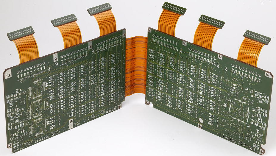
Tooling holes need to be placed with the fixture in mind, since the board position is set by those holes and by the fiducials the fixture recognises. Tolerance in the hole position translates directly into probe misalignment.
Test Point Numbering and Documentation
Every test point should have a unique identifier that appears in the schematic, the layout and the fixture documentation. The net name alone is ambiguous where several nets share a name, and a fixture built from the wrong list is expensive to correct.
Include a test point layer in the fabrication and assembly drawing package, and state the pad size, the side, and any probe access restrictions. The assembly house and the fixture builder both work from that data, and ambiguity between them produces a fixture that fits the drawing but not the board.
Reviewing Placement Before Release
Review test point placement as a separate pass, after the copper is stable and before the artwork is released. Check clearances, sizes, side access and coverage against the test plan, and confirm that no test point sits where a component will later be placed.
gopcb reviews test access with customers when a design pushes spacing or pad size limits, because a design that cannot be tested economically will be tested by hand at a much higher cost per unit, which is rarely a quality improvement.
Points to Confirm at First Article
Consumables have a life measured in cycles, and the replacement point should come from the measurement rather than from a failure.
FAQ
How large should a test point pad be? For standard probes, 1.2 to 1.5 millimetres is a practical working size. Smaller pads need finer probes, more precise fixtures and more maintenance.
Can I use vias as test points? Yes, provided the annular ring is adequate and the via is not tented. Confirm the surface finish is solderable or at least probe friendly, and check that the probe travel is not obstructed.
Do test points hurt high speed signals? They add capacitance and a stub, which can cause reflections. Keep the stub short, avoid probing differential pairs asymmetrically, and use flying probe or boundary scan where the signal is very fast.