Thermally Conductive PCB: How the Dielectric Layer Works
A thermally conductive laminate is built around a simple idea: replace the glass-reinforced dielectric with something that carries heat far better, so that the components on the board have a short path to a metal structure. The important word is laminate, because the material is processed like any other circuit substrate rather than being a metal plate with electronics attached. Understanding the layer structure explains both what the material can do and where its limits lie.
The Layer Structure
Four layers make up the stack. At the bottom is a metal base, usually aluminium and occasionally copper. Above it sits a thermally conductive dielectric, typically between seventy five and a hundred and fifty micrometres thick. On top of that is the circuit copper, and over the circuit is the solder mask and the surface finish.
The dielectric is the interesting layer. It has to be electrically insulating while being a reasonably good conductor of heat, and those two requirements pull in opposite directions because most good insulators are poor conductors. The materials achieve it by loading a polymer with ceramic particles, usually alumina or boron nitride, which raises the thermal conductivity to several times that of ordinary laminate while keeping the dielectric strength high enough for the application. Where the circuit requires higher isolation, the dielectric is made thicker, which raises the thermal resistance in direct proportion.
Why the Dielectric Layer Controls Everything
The thermal resistance of the board is dominated by the dielectric, because it is thin but has by far the lowest conductivity in the stack. A typical value might be a few tenths of a degree per watt for a small area, which sounds insignificant until it is compared with the junction to case resistance of the device mounted on it.
That comparison is the design calculation. If the device has a junction to case resistance of one degree per watt and the board adds three, then the board is the limiting element and improving the device will achieve nothing. Reducing the dielectric thickness, increasing the copper area of the pad above it, or moving to a filled material with higher conductivity are the only options, and each has a cost or a voltage penalty. Our copper core article describes how the alternative construction compares.
Heat Spreading and the Metal Base
The metal base does not conduct heat away by itself; it spreads it. Heat that arrives at a point under a component would otherwise raise the local temperature until the surrounding material carried it away, and the metal base turns that point source into a distributed source over the whole board area.
Spreading only works if the heat has somewhere to go. A board mounted in free air with no thermal connection to a structure simply reaches a higher equilibrium temperature, because the spreading has reduced the local hot spot but the total dissipation is unchanged. The benefit appears when the board is bolted to a metal housing or a heat sink, which is why a thermally conductive board is chosen together with a mechanical design that provides a heat path, not as a substitute for one.
Manufacturing the Stack
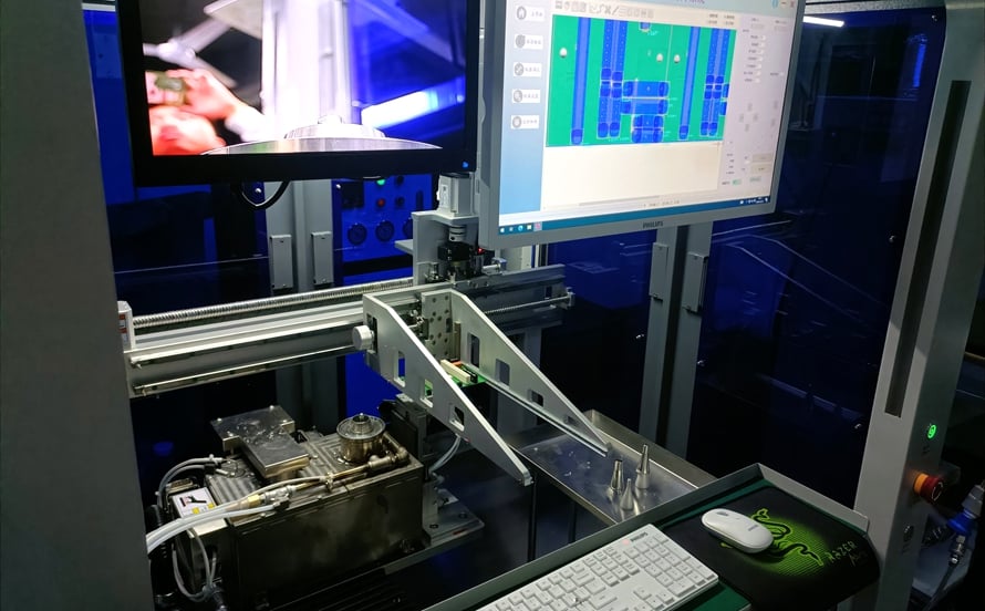
Fabrication follows the same sequence as a conventional single sided board with a few differences. The metal base is machined or punched to shape, the dielectric is laminated onto it under heat and pressure, and the circuit copper is bonded on top. Holes are drilled through the whole stack, and because the base is a solid conductor, plated interconnections between the two faces are not possible in the usual way.
Two consequences follow. The first is that most designs are single sided, since there is no way to route a signal from one face to the other. The second is that the mechanical tolerance of the metal base becomes part of the electrical design, because the base is often the mounting surface and its flatness affects how well the assembly transfers heat into the structure. Our thermal management article describes how the interface between the board and the housing is specified.
Electrical Behaviour of the Dielectric
A filled dielectric is not equivalent to an ordinary laminate electrically. Its dielectric constant is typically higher, which means narrower traces for a given impedance, and it varies more with frequency because the filler and the polymer behave differently. For a circuit that carries only power and low frequency signals, this is irrelevant. For a circuit that also carries high speed or radio frequency signals, the impedance has to be calculated for the actual material rather than assumed.
The dielectric strength is the other electrical parameter that matters. It determines the voltage the board can withstand between the circuit and the base, and it falls as the layer is thinned for thermal reasons. Where the circuit includes mains voltages, the requirement is usually the factor that sets the thickness, and the thermal design then has to work within that constraint rather than choosing the thinnest available layer.
Applications and Selection
LED lighting dominates the volume, because the emitters dissipate most of their input as heat and the board is the natural path into the luminaire housing. Power conversion follows, where the thermal limit rather than the electrical one sets the maximum current, and motor drives and solid state relays use the same reasoning.
Selection comes down to three questions. What is the maximum junction temperature and the dissipation, which sets the required thermal resistance. What is the isolation voltage, which sets the dielectric thickness. And what is the mechanical arrangement, which determines whether the base can actually transfer its heat. Answering those three usually identifies a single construction, and the choice between aluminium and copper then follows from the thermal demand. Our design release checklist places those questions in the review sequence.
Where the Material Reaches Its Limit
These materials improve the path from a component into the structure, but they do not create a path where none exists. A board that is mounted on standoffs in open air still has to reject its heat by convection and radiation, and the metal base only makes the board surface larger and more uniform. The improvement in that case is modest, and a designer who expects a dramatic reduction in temperature without a mechanical heat path will be disappointed.
The second limit is the isolation requirement. Where the circuit operates from the mains, the dielectric thickness is set by the safety standard rather than by the thermal calculation, and the resulting thermal resistance may be three or four times what a thin layer would offer. In that situation the options are to increase the copper area, to reduce the dissipation, or to accept a lower ambient rating for the product, and the thermal calculation should be done with the thicker layer from the start.
FAQ
Is a thermally conductive laminate the same as a metal core board? The terms overlap heavily in practice. Both use a metal base with a filled dielectric, and the differences are in the specific materials and their rated thermal conductivity.
Can these boards be multilayer? Yes, with a dielectric and a copper layer on both faces of the metal base, but the cost rises sharply and the mechanical benefit is unchanged, so it is only done when the routing genuinely requires it.
Why does the dielectric thickness matter so much? Because it is both the dominant thermal resistance and the isolation barrier. Thinner transfers heat better and isolates less, so the two requirements have to be balanced explicitly rather than by default.