PCB Manufacturing Services: Process, Lead Time, Quality
PCB manufacturing services are the bridge between a design file and a physical board, and the quality of that bridge decides whether a product ships on schedule. Two suppliers can quote the same Gerber package and deliver boards that behave very differently, because fabrication is a chain of chemical and mechanical steps where small process differences accumulate. This article walks through what the service actually does, where lead time comes from, and which quality factors are worth checking before a program commits to volume.
What the Service Actually Delivers
The deliverable is a bare board built to the supplied data, and the wider design and fabrication flow sets what that data has to contain: Gerber or ODB++ artwork, drill files, and a stackup drawing. The supplier translates those into panel images, selects laminate and prepreg, runs the process, and tests the result. Materials are usually FR-4, with aluminum or metal-core substrates for LED and power work and low-loss laminates for RF. Two-layer prototypes and twelve-layer high-speed boards come off the same service, but not off the same process window, and that difference drives both price and schedule.
The Fabrication Sequence
Inner-layer imaging comes first on a multilayer job. Photoresist is laminated to copper-clad laminate, exposed through film, developed, and etched to leave the conductor pattern. The etched inner cores are then inspected and oxide-treated so the resin will bond to them.
Lamination stacks the cores with prepreg between them and presses the book under heat and pressure until the resin flows and cures. The result is a rigid panel with the inner layers locked in place and registration holes to align everything that follows.
Drilling then opens the vias. Mechanical drilling covers most through holes; laser drilling forms microvias on HDI work. After drilling, a desmear step cleans resin residue out of the barrel so plating can bond.
Plating deposits copper through the holes and across the surface. Electroless copper seeds the barrel, and electrolytic plating builds it to the specified wall thickness, typically 20 to 25 micrometres. Outer-layer imaging and etching then define the outer conductors.
Solder mask is applied, exposed, and developed to open the pads. Surface finish follows, then legend printing, then routing or punching to the final outline.
Electrical test closes the loop. Flying-probe or fixture test checks every net for opens and shorts, and optical inspection catches the visual defects that electrical test cannot see.
Where Lead Time Comes From
Standard lead time for a routine multilayer board is five to seven working days from data release. Expedited service compresses that to 24 to 72 hours and is charged accordingly. Complex or HDI work with stacked microvias and multiple lamination cycles runs ten to fifteen days and sometimes longer.
Four variables decide where a job lands in that range. Layer count is the largest, because each additional lamination cycle is a distinct process pass. Material availability is the second: a standard FR-4 grade is stocked, while a specific low-loss laminate or an unusual thickness has to be ordered. Surface finish is the third, since some finishes are batch processes on a fixed schedule. Testing scope is the fourth: adding X-ray inspection of barrel quality or a full flying-probe pass adds time at the end of the line.
Quoted lead time usually starts when the data is confirmed as manufacturable, not when it is emailed. That distinction matters most on expedited orders, where a day lost to an engineering query cannot be recovered.
What Separates Good Quality from Average
Material provenance is the first factor, and it is invisible in the finished board. Certified laminate from a known source behaves predictably through thermal cycling; unverified material can pass incoming inspection and still fail in the field. The specification and country of origin should be documented, especially for products carrying safety or automotive approvals.
Conductor tolerance is the second. A well-controlled line holds trace width and spacing within about 0.05 mm of the design, which matters most on impedance-controlled nets, where a small width shift moves the characteristic impedance.
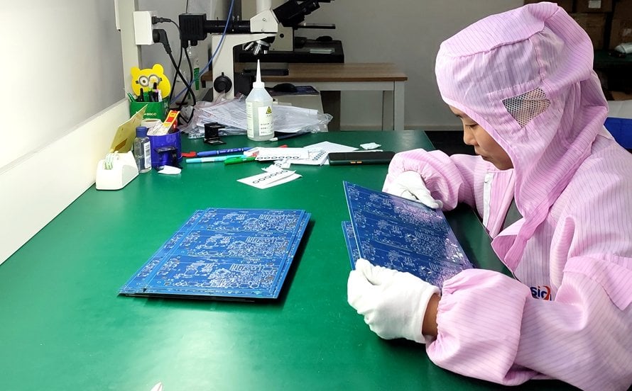
Process environment is the third. Cleanroom conditions for mask and imaging steps reduce the particulate contamination that causes shorts and blistering. This is not visible on a datasheet and is one of the main reasons two apparently similar shops produce different yields.
Inspection capability is the fourth. Optical inspection finds pattern defects, X-ray confirms barrel plating in dense arrays, and flying probe or fixture test verifies electrical continuity. A supplier with all three catches problems before shipment rather than at the customer assembly line. Documented quality control, along with the quality characteristics that matter downstream, is what separates a certificate on a wall from a process that actually holds tolerance.
Certifications Worth Checking
Quality management certification is the baseline. ISO 9001 covers the management system. UL recognition matters for boards that will carry a safety listing. RoHS compliance is a requirement for most consumer and industrial markets, and it must be documented rather than assumed, because it depends on the specific material set used. Automotive programs typically require IATF 16949, which adds traceability and change-control discipline. The IPC performance classes, Class 2 for general industrial and Class 3 for high-reliability applications, define the inspection standard the board is built to. Asking which class a supplier runs by default is more informative than asking whether it supports Class 3.
Comparing Suppliers
Start with capability, stated in numbers: maximum layer count, minimum line width and spacing, minimum drill diameter, maximum panel size, and the smallest via the line holds in production. A supplier that quotes a capability it does not run routinely will produce a good first article and inconsistent volume.
Delivery capability comes next. Can the shop support a fast prototype and then scale to volume without changing process, material, or factory? A supplier that prototypes one way and produces another introduces a transfer risk that is expensive to discover late, which is why the PCBA development process is worth mapping before the first order.
Technical support is the third factor and is often undervalued. Free design-for-manufacturability review, or DFM analysis, catches the problems that cost the most to fix: a stackup that cannot be drilled, a footprint that cannot be soldered, a panel that wastes material. A supplier that raises these questions before building is worth more than one that simply builds what it was sent.
Order flexibility is the fourth. A supplier that accepts a small pilot lot and then scales into production lets a program validate the process before committing to a large purchase order, which is the cheapest form of risk reduction available.
How the Price Structure Works
Board pricing is a function of layer count, board area, quantity, surface finish, and any special process. A ten-piece order of two-layer FR-4 boards around 100 by 100 mm typically lands between 25 and 40 dollars. Five four-layer boards at 50 by 50 mm with ENIG finish commonly run 60 to 90 dollars. Ten six-layer impedance-controlled boards move into the 120 to 180 dollar range. A single two-layer aluminum board is usually 12 to 18 dollars. An eight-layer HDI build with blind and buried vias and laser-drilled microvias can exceed 250 dollars for a single order. Volume discounts of 30 to 50 percent against prototype pricing are normal once quantities reach the thousands, and quotes usually exclude freight and taxes.
Balancing Cost, Speed, and Quality
The lowest quote is rarely the cheapest outcome. A board that arrives a week late, or that fails at assembly because of a plating defect, costs far more than the price difference between two suppliers. The pattern that works is to prototype with the supplier that will eventually build volume, verify the process on real boards rather than on samples alone, and confirm that engineering communication stays responsive as quantities grow.
FAQ
How long does PCB manufacturing take? Five to seven working days is standard for a routine multilayer board, 24 to 72 hours for expedited service, and ten to fifteen days for complex or HDI designs.
What data do I need to send? Gerber or ODB++ artwork, an NC drill file, a stackup drawing, and any impedance requirements. RS-274X is the most widely accepted Gerber format.
Which certifications should a supplier hold? ISO 9001 as a baseline, UL recognition for safety-listed products, RoHS documentation for most markets, and IATF 16949 for automotive programs.
Is expedited service worth the premium? Only when schedule genuinely dominates. Expedited charges exist because the board jumps the queue and uses reserved capacity, and they are hard to justify for a prototype that is not on a critical path.