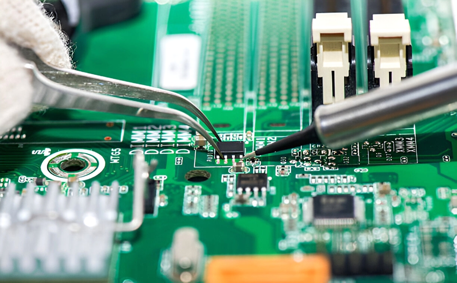
At Kingda, we provide reliable and professionally controlled Through-Hole PCB Assembly solutions for electronic products that require strong mechanical connections, dependable solder joints, and long-term operating stability. Through-hole technology remains an important assembly method for applications involving large components, high mechanical stress, high-current connections, or components that are frequently subjected to vibration and thermal cycling.
Our PCB Assembly capabilities can support products ranging from prototypes and low-volume builds to higher-volume production. Depending on product requirements, through-hole components can be assembled on single-sided, double-sided, or multilayer PCBs and can also be integrated with surface-mount technology (SMT) to create hybrid assemblies.
By combining established THT processes with modern inspection and process-control methods, Kingda helps customers achieve consistent assembly quality while balancing manufacturability, reliability, and production cost.
What Is Through-Hole PCB Assembly?
Through-Hole PCB Assembly is a PCB assembly method in which electronic components are mounted by inserting their leads through holes drilled in the printed circuit board. The component leads extend through the board and are soldered to conductive pads, typically on the opposite side.
Unlike surface-mount components, which are soldered directly to pads on the PCB surface, Through-Hole Components are mechanically anchored through the board. This structure provides excellent mechanical strength and makes through-hole technology particularly suitable for components exposed to vibration, mechanical loads, repeated insertion forces, or high electrical currents.
The holes used for through-hole assembly are generally plated through-holes (PTHs). The hole diameter must be properly matched to the component lead diameter and manufacturing tolerance to ensure reliable insertion while maintaining sufficient annular ring and solderability.
Through-hole assembly can be performed manually or with automated equipment. In modern production, automated insertion, selective soldering, wave soldering, automated optical inspection, and electrical testing may be combined to improve consistency and manufacturing efficiency.
Common Lead Configurations for THT Components
Through-Hole Components are available in many package and lead configurations. Two common lead arrangements are axial and radial.
- Axial leads: The leads extend from opposite ends of the component body along the same axis. Resistors, diodes, and some inductors are common examples of axial components.
- Radial leads: The leads generally extend from the same side of the component body. Capacitors, LEDs, transistors, and many connectors use radial lead configurations.
Dual in-line packages (DIP) are another well-known through-hole package type. DIP components contain two parallel rows of leads designed to fit into corresponding PCB holes. Their standardized pitch and robust mechanical structure have made them widely used in conventional electronic assemblies and development platforms.
Through-Hole PCB Assembly Process
The specific manufacturing sequence depends on the PCB design, component mix, production volume, and whether the board also contains SMT components. A typical THT Assembly process includes component preparation, insertion, soldering, cleaning when required, inspection, and testing.
Step 1: Component Preparation and Insertion
The first step is to prepare and insert the components into the PCB’s designated holes.
Components may be inserted manually or by using automated insertion equipment. Automated equipment can improve placement consistency and production efficiency, particularly when a product contains a large number of repeated axial or radial components.
Before insertion, manufacturers should verify:
- Component part numbers and specifications
- Component orientation and polarity
- Lead diameter and length
- Hole diameter and pitch
- Component body dimensions
- Insertion direction
- PCB revision and assembly documentation
Proper component preparation is important because incorrect orientation or part placement can result in electrical failures that may not be immediately visible during visual inspection.
Step 2: Wave Soldering
Wave Soldering is one of the most widely used soldering processes for through-hole assemblies. During this process, the PCB is transported over a controlled wave of molten solder. Component leads extending through the PCB contact the solder wave, allowing solder to form joints between the leads and plated-through-hole pads.
A typical wave soldering process includes several stages:
- Flux application: Flux is applied to help remove surface oxides and improve solder wetting.
- Preheating: The PCB is gradually heated to activate the flux and reduce thermal shock.
- Soldering: The bottom side of the PCB passes through a controlled molten solder wave.
- Cooling: The assembly is cooled under controlled conditions to stabilize the solder joints.
Process parameters such as solder temperature, conveyor speed, preheat temperature, flux quantity, board orientation, and contact time must be controlled carefully. Improper settings can lead to insufficient soldering, solder bridges, voids, dewetting, or component movement.
For mixed SMT and THT assemblies, selective soldering can be used when only specific through-hole locations need to be soldered. This approach can reduce the risk of exposing temperature-sensitive or nearby SMT components to unnecessary soldering conditions.
Step 3: Cleaning
Flux residues remaining after soldering may require cleaning depending on the flux chemistry, product requirements, and reliability environment.
Cleaning may be performed using appropriate aqueous, solvent-based, or other validated processes. However, not every PCB requires complete cleaning. No-clean fluxes, for example, are designed to leave residues that can remain on the board when the manufacturer’s process and end-use requirements permit.
When cleaning is necessary, the process should remove residues without damaging components, solder joints, coatings, labels, or sensitive materials. The cleaned PCB should also be properly dried before subsequent inspection and testing.
Step 4: Inspection and Testing
After soldering and cleaning, the assembled PCB should undergo inspection and, when required, electrical or functional testing.
Inspection methods may include:
- Visual inspection
- Automated optical inspection (AOI)
- X-ray inspection for selected applications
- Continuity and resistance testing
- In-circuit testing (ICT)
- Functional testing
Inspection criteria should be established according to the PCB design, customer requirements, and applicable industry standards.
Benefits of Through-Hole PCB Assembly
Although SMT has become the dominant assembly technology for many modern electronic products, PTH Assembly remains highly valuable for specific applications. Its mechanical and electrical characteristics provide several important advantages.
Strong Mechanical Reliability
One of the major advantages of Through-Hole PCB Assembly is its strong mechanical connection.
Because component leads pass through the PCB, the soldered connection is mechanically supported by the board structure. This makes through-hole components well suited to applications exposed to vibration, shock, mechanical stress, or repeated physical loads.
Large connectors, transformers, power components, switches, and other mechanically demanding components are often good candidates for through-hole mounting.
Suitable for High-Current Applications
Through-hole packages can accommodate components with relatively large leads and robust terminals. This makes them useful in certain power electronics and high-current applications.
However, current-carrying capability depends on the complete electrical design, including copper thickness, trace width, thermal conditions, via structure, component terminals, and allowable temperature rise. Therefore, component mounting technology alone does not determine current capacity.
Easier Prototyping and Manual Rework
Through-hole components can be convenient for prototypes, engineering samples, and certain repair or rework operations.
Technicians can often remove and replace individual components using conventional soldering and desoldering equipment. This can simplify development and troubleshooting when component changes are expected during the design-validation stage.
Robust Component Mounting
Through-hole mounting provides strong physical retention and can be particularly useful for relatively large or heavy components.
Components such as connectors, relays, transformers, inductors, switches, and some capacitors may benefit from the additional mechanical support provided by through-hole mounting.
Integration With SMT
Modern electronic products do not necessarily have to choose between SMT and THT. Many designs use a hybrid PCB Assembly approach in which miniature SMT components are placed on the PCB surface while mechanically or electrically demanding components are installed using through-hole technology.
This combination allows designers to balance board density, mechanical strength, thermal performance, and component availability.
Challenges of Through-Hole PCB Assembly
Despite its advantages, THT Assembly also presents several manufacturing challenges.
Larger PCB Area Requirements
Through-hole components generally require larger mounting areas than comparable SMT components because the PCB must accommodate drilled holes and through-hole pads.
For high-density electronic products, excessive use of THT components can reduce available routing space and increase PCB dimensions.
Additional Drilling Requirements
PTH assembly requires accurately drilled and plated holes. Hole diameter, positional tolerance, plating quality, and annular ring dimensions must be considered during PCB design and manufacturing.
Poor hole design can lead to difficult component insertion, damaged leads, insufficient solder coverage, or reduced mechanical reliability.
Component Lead Deformation
Component leads can become bent or deformed during transportation, insertion, or handling. Excessive lead deformation may make automated insertion difficult or result in incorrect component placement.
Proper component packaging, handling, insertion-force control, and lead preparation can help reduce these problems.
Wide Variety of Component Packages
THT components are available in many body shapes, lead configurations, dimensions, and insertion requirements. Managing different component types can therefore increase production complexity.
Manufacturers need accurate bills of materials (BOMs), assembly drawings, polarity information, component specifications, and process instructions to maintain consistency.
Labor and Ergonomic Considerations
Manual insertion and soldering can increase labor requirements, especially for products with many through-hole components.
For high-volume production, automated insertion and soldering technologies can reduce repetitive manual work and improve process consistency. For prototypes and low-volume products, however, manual assembly may remain practical depending on the product structure.
Applications of Through-Hole PCB Assembly
PTH Assembly is still widely used in electronic products where mechanical strength, component size, or electrical requirements make through-hole mounting advantageous.
Industrial Electronics
Industrial control systems, robotics, motor controllers, sensors, instrumentation, power supplies, and automation equipment may use through-hole components.
Industrial products often operate under vibration, temperature fluctuations, and long service cycles, making mechanically robust component mounting valuable.
Aerospace and Defense Electronics
Aerospace and defense systems can contain large connectors, power components, transformers, and other components that require strong mechanical attachment.
However, aerospace and defense applications also involve strict requirements for materials, traceability, environmental performance, reliability, and testing. The appropriate assembly technology must therefore be selected according to the complete system specification.
Consumer and Commercial Electronics
Although many compact consumer devices rely primarily on SMT, through-hole technology continues to appear in products that use large connectors, switches, transformers, power components, or mechanically stressed components.
Certain audio equipment, industrial consumer products, power devices, and development platforms may use a combination of SMT and THT.
Automotive Electronics
Automotive electronic systems can use through-hole components in applications where mechanical robustness and reliable connections are important.
Examples may include control modules, power circuits, connectors, sensors, and other assemblies. In many cases, automotive products use hybrid SMT/THT assembly to balance miniaturization with mechanical and electrical requirements.
Common Defects in PTH Assembly
Maintaining stable process parameters is essential for reliable PTH Assembly. Common defects include:
Component Lifting
Component lifting can occur when a component moves during soldering or when lead geometry is inconsistent.
Factors such as lead length, lead stiffness, component fit, PCB orientation, and soldering conditions can influence component movement.
Proper lead preparation, insertion control, and soldering-process optimization can reduce the risk.
Missing Components
A missing component occurs when a required component is absent from its designated PCB location.
Possible causes include:
- Incorrect component loading
- Insertion-machine errors
- Manual insertion mistakes
- Component shortages
- Incorrect assembly instructions
Automated inspection and production-line verification can help detect missing components before the board proceeds to later stages.
Incorrect Component Orientation
Polarity-sensitive components such as diodes, electrolytic capacitors, LEDs, and some semiconductor devices must be installed in the correct orientation.
Incorrect orientation can cause immediate electrical failure or create reliability problems during operation.
Clear PCB markings, assembly drawings, component identification, and automated inspection can significantly reduce orientation errors.
Solder Bridging
Solder bridging occurs when excess solder connects two or more electrically separate conductors.
It can result from excessive solder volume, unsuitable lead spacing, incorrect wave-soldering parameters, PCB design issues, or component placement conditions.
Controlling solder temperature, wave height, conveyor speed, pad design, and component spacing can help minimize this defect.
Insufficient Solder
Insufficient solder can reduce mechanical strength and electrical conductivity.
It may result from inadequate solder contact, poor wetting, insufficient flux activity, incorrect solder-wave parameters, or unfavorable PCB/component geometry.
Process monitoring and visual or automated inspection are important for identifying insufficient solder joints.
Voids and Poor Wetting
Voids are internal gaps within a solder joint, while poor wetting occurs when molten solder does not properly spread across the intended surfaces.
The severity and acceptance criteria depend on the component type, solder joint geometry, and application requirements. Optimizing flux application, preheating, solder temperature, and board design can improve solderability.
How to Detect and Prevent PTH Assembly Defects
Effective quality control should combine defect detection with process prevention.
Inspection and Verification
Inspection can be performed manually or automatically depending on product complexity and production volume.
AOI can compare the assembled board against defined inspection criteria and help identify missing components, incorrect orientations, solder bridges, and other visible assembly problems.
For solder joints or structures that cannot be adequately evaluated through optical inspection, X-ray inspection may be appropriate for selected applications.
Electrical testing can provide another level of verification by checking continuity, resistance, shorts, open circuits, and other electrical characteristics.
Process Monitoring
Inspection alone is not enough. Manufacturers should also monitor the processes that generate defects.
Important parameters may include:
- Component insertion accuracy
- Lead condition
- Flux application
- Preheat temperature
- Solder temperature
- Conveyor speed
- Wave height
- Solder contact time
- Cleaning conditions
- Inspection results
Tracking defect trends can help identify recurring problems before they affect a large production batch.
Root Cause Analysis
When defects occur repeatedly, manufacturers should investigate the underlying cause instead of simply repairing individual boards.
A Pareto analysis can be used to identify the most frequent defect categories. Engineers can then investigate possible causes related to PCB design, component quality, machine settings, materials, operator procedures, or process variation.
Corrective and preventive actions should be documented and verified to ensure that the issue does not recur.
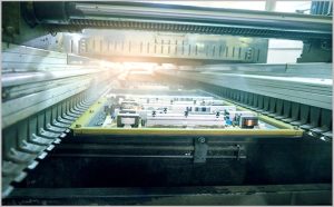
Design Considerations for Through-Hole PCB Assembly
Good PCB Manufacturing results begin with a design that considers assembly requirements from the beginning.
Designers should pay attention to:
- Hole diameter and component lead tolerance
- Pad and annular-ring dimensions
- Component spacing
- Component orientation
- Soldering access
- Copper distribution
- Thermal relief design
- PCB thickness
- Component height
- Mechanical clearance
- Mixed SMT/THT placement
- Inspection accessibility
Design for manufacturability (DFM) analysis can identify potential problems before production begins. This helps reduce rework, improve assembly yield, and simplify the transition from prototype to mass production.
Through-Hole Assembly vs. SMT Assembly
| Feature | Through-Hole Assembly | SMT Assembly |
|---|---|---|
| Component mounting | Leads pass through PCB holes | Components mount directly on PCB pads |
| Mechanical strength | Generally high | Depends on package and solder-joint design |
| Component size | Often larger | Suitable for compact components |
| PCB space | Requires drilled holes and additional area | Better suited to high-density layouts |
| Automation | Automated insertion and soldering available | Highly automated |
| Prototyping/rework | Convenient for many conventional components | Requires appropriate rework tools |
| Typical applications | Connectors, power components, mechanically stressed parts | High-density digital, consumer, communication, and compact electronics |
In many modern products, the most effective solution is not to select only one technology. Hybrid assembly can combine SMT’s high density with THT’s mechanical robustness and suitability for larger components.
Quality Control for Through-Hole PCB Assembly
Reliable PCB Assembly requires quality control throughout the entire manufacturing process rather than relying only on final inspection.
A comprehensive quality approach may include:
- Incoming material verification to confirm component identity and PCB specifications.
- Component preparation control to prevent incorrect parts and damaged leads.
- Insertion verification to ensure correct location and orientation.
- Soldering-process monitoring to maintain stable process parameters.
- Visual and automated inspection to detect assembly defects.
- Electrical testing to identify open circuits, shorts, and functional problems.
- Traceability and documentation to support production analysis and corrective actions.
Applicable IPC requirements and customer-specific acceptance criteria should be incorporated into the inspection and manufacturing plan according to the intended application.
Choosing a Through-Hole PCB Assembly Partner
When selecting a PCB Manufacturing and assembly partner, companies should evaluate more than price alone.
Important factors include:
- Experience with THT and hybrid SMT/THT production
- Component insertion capabilities
- Wave and selective soldering capabilities
- Inspection and testing resources
- DFM support
- Component and BOM management
- Process traceability
- Quality-control procedures
- Prototype and production-volume flexibility
- Ability to support the required PCB materials and structures
For projects requiring both surface-mount and through-hole components, it is particularly important to select a manufacturer that understands the interaction between PCB design, component placement, soldering processes, and inspection requirements.
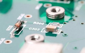
Through-Hole PCB Assembly Services at Kingda
Kingda provides Through-Hole PCB Assembly solutions for products that require robust component mounting and reliable solder connections. Through-hole assembly can be incorporated into different PCB structures and can also be combined with SMT technology when the product requires a hybrid manufacturing approach.
Our assembly process focuses on controlled component placement, soldering consistency, inspection, and manufacturing quality. By evaluating PCB design, component characteristics, and production requirements together, Kingda can help customers develop an assembly process that is practical for both prototypes and production builds.
For projects involving connectors, power components, industrial electronics, control systems, automotive electronics, or other mechanically demanding assemblies, THT can provide an effective complement to modern SMT manufacturing.
Conclusion
Through-Hole PCB Assembly remains an important electronic manufacturing technology despite the widespread adoption of SMT. Its strong mechanical attachment, suitability for larger components, and compatibility with high-current or mechanically demanding applications make it a practical choice for many products.
A reliable THT Assembly process requires more than simply inserting components and applying solder. Hole design, component preparation, insertion accuracy, flux application, Wave Soldering, inspection, electrical testing, and process control all contribute to final assembly quality.
For products that combine high-density SMT components with mechanically robust through-hole components, hybrid PCB assembly can provide an effective balance between miniaturization, reliability, manufacturability, and cost. With appropriate DFM planning and process control, Kingda can support reliable through-hole and mixed-technology assembly solutions for a wide range of electronic applications.