PCB Design Review: Mistakes That Cost a Revision
Most board revisions are not caused by a circuit that did not work. They are caused by details that were never checked: a footprint with the wrong pad pitch, a connector placed where the enclosure will not let the cable bend, a test point hidden under a component, or a thermal pad with nowhere for the heat to go. A structured PCB design review catches these before tooling is committed, and it costs a morning rather than a week.
Start With the Footprints
Footprints are the most common source of expensive rework because they are copied from libraries without verification. A pad pitch that is slightly wrong prevents the part from seating at all, and an incorrect courtyard lets components overlap on the assembly drawing. Every new footprint should be checked against the manufacturer drawing, including the pad sizes, the pitch, the thermal pad geometry and the polarity markings.
The check should also cover the paste layer. A thermal pad that is covered completely with paste lifts the part during reflow, and a pad that is divided into a grid of small apertures releases more reliably. Where the part is a fine pitch package, the stencil aperture, the solder mask opening and the copper pad should be reviewed together rather than separately. Our notes on PCB design quality characteristics list the checks that belong in this stage.

Clearance, Copper and Thermal Relief
Clearance violations are caught by a design rule check, but the rules themselves have to be right. Minimum spacing should follow the fabrication capability and the electrical requirement for the working voltage, and it has to be achievable at the corners and in dense areas rather than only in the open regions of the board. A rule that passes on average and fails locally is worse than no rule at all.
Thermal relief deserves a specific review. A pad connected to a large plane by solid copper is difficult to solder because the plane conducts the heat away faster than the iron can supply it, so a thermal relief pattern with spokes is used instead. Where the pad carries current as well as heat, the relief has to be wide enough not to become the bottleneck, and that trade is worth checking explicitly on power components.
Test Access and Programming
Every net that cannot be reached through a connector should have a probe point, and the point should be free of components so that a fixture can seat. Where a bed of nails will be used, the test points should be on a consistent pitch, kept away from tall parts, and positioned so that the fixture does not need to press on a connector or a fragile component.
Programming and debugging access is part of the same review. A header that is inaccessible once the enclosure is fitted turns every firmware change into a disassembly, and a debug interface shared with a functional pin needs a deliberate decision about how the two coexist in production. Planning the access at layout time costs a few square millimetres; adding it later costs a revision.
Silkscreen, Mask and Assembly Information
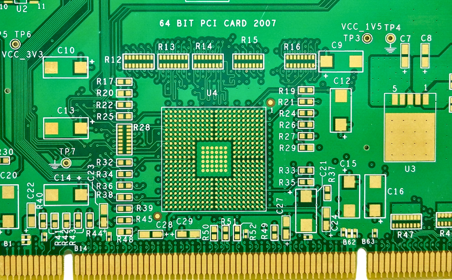
Silkscreen is documentation, and it should be reviewed as such. Reference designators must match the bill of materials, polarity marks must be unambiguous, and pin one indicators must be on the correct end of the footprint. Where the board is dense, silkscreen should be trimmed rather than allowed to sit over a pad, because ink on a pad interferes with soldering and is a rejection criterion in many assembly standards.
Solder mask and paste mask layers need the same attention. A mask opening that is too small encroaches on the pad, one that is too large exposes traces, and a paste aperture that is oversized deposits too much solder and encourages bridging. Reviewing the three layers against the component drawing catches most assembly defects before they appear on a line.
Mechanical Fit and Enclosure
The board has to fit the product, and that means more than the outline. Component heights must clear the lid, connectors must align with the apertures in the case, and mounting holes must match the bosses and the screw heads that will sit in them. Where a board is retained by clips or rails, the edge clearance has to account for the tolerance of the moulding as well as of the board.
It is worth checking the connectors against the cable as well. A cable that must bend immediately behind a connector will strain the joint unless there is room, and a connector that must be mated by hand needs sufficient space around it for fingers or a tool. Our notes on board outline and mounting design cover the mechanical details.
Electrical Checks Worth Doing by Hand
Some checks are not automated. The return path under the fastest nets should be traced by eye, because a plane split that the tool does not flag can still interrupt it. The decoupling should be checked against the pin it serves rather than against the schematic, and the crystal should be reviewed with its load capacitors in place, since a crystal placed far from the device or over a noisy plane will not oscillate reliably.
The power stage deserves its own pass. The switching loop, the current sense return and the gate drive path should all be traced on the layout, and the copper widths checked against the current rather than against the previous design. Our notes on the PCB design process show where these checks fit into the wider flow.
Running the Review as a Process
A review works better with an agenda than with an open invitation to comment. Assign each area to a named person, give them the relevant drawing and a checklist, and ask for findings in writing. The author should not be the only reviewer of their own layout, and a reviewer who has not seen the schematic is often the most useful because they read what is actually drawn rather than what was intended.
The output should be a list of issues with a decision for each: fix, accept with a reason, or defer to a later revision. Recording the accepted risks is as important as recording the fixes, because it stops the same discussion recurring on the next project and gives the team a written basis for the trade-offs that were made.
Documents to Review Alongside the Layout
The layout cannot be reviewed in isolation. The stackup drawing, the fabrication notes, the assembly drawing and the bill of materials all have to agree with it, and a mismatch between them is a defect even when each document is internally consistent. Checking the revision numbers on all four at the same time prevents the classic failure where a stackup was updated and the layout was not.
Where the design includes a new process step, such as a filled via, a press fit pin or a selective finish, the requirement should be written down rather than implied by the layout geometry. Suppliers build to documents, not to intentions, and an unstated requirement is one that will be interpreted differently by each quotation. Our notes on PCB manufacturing tolerances give the numbers that belong in those notes.
FAQ
What is the most common cause of a board revision? Footprint and mechanical errors rather than electrical ones. A wrong pad pitch, a misplaced connector or a component that fouls the enclosure accounts for a large share of first article failures.
Who should review a PCB layout? Someone other than the author, ideally including one person who has not seen the schematic, since they will judge what is drawn rather than what was intended. A hardware engineer and a manufacturing engineer make a useful pair.
How long should a review take? A structured review of a moderate board takes a few hours. That is far less than the cost of a revision, and it is the cheapest engineering time in the whole project.