Via in Pad Design and Paste Escape for Thermal Pads
Via in pad means placing a plated hole directly inside a surface mount land so that the pad serves both as a solder site and as a vertical connection, and it is the standard way to move heat out of a power package. The technique only works when the hole is filled and capped properly, because an open barrel underneath a pad will pull the paste away from the joint as it melts.
What Via in Pad Actually Solves
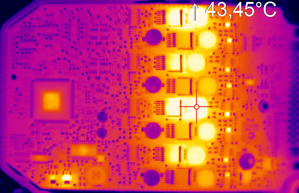
The technique exists because a power device has to get rid of heat through the board rather than through the air. A thermal pad on the underside of a package sits over an array of small holes that carry energy into the copper planes below, and those holes have to sit inside the land rather than beside it to keep the thermal path short.
It is also used to free routing space. A via placed inside a pad removes the short stub of trace that a conventional fanout needs, which matters on a fine pitch package where two traces have to escape from between adjacent pads and any extra millimetre of copper blocks the channel.
Why Solder Wicking Happens
An open hole is a capillary, and molten solder is drawn into it by the same force that lifts oil up a wick. The paste printed over the hole melts first at the edges, then flows down the barrel, leaving a void in the joint and a solder deposit on the far side of the board.
Wicking is worse when the hole is large, when the paste volume is generous, and when the board is heated slowly enough for the solder to stay liquid for a long time. It also gets worse when the far side of the hole is open, because there is nothing to stop the solder travelling through.
Tenting, Plugging and Filling
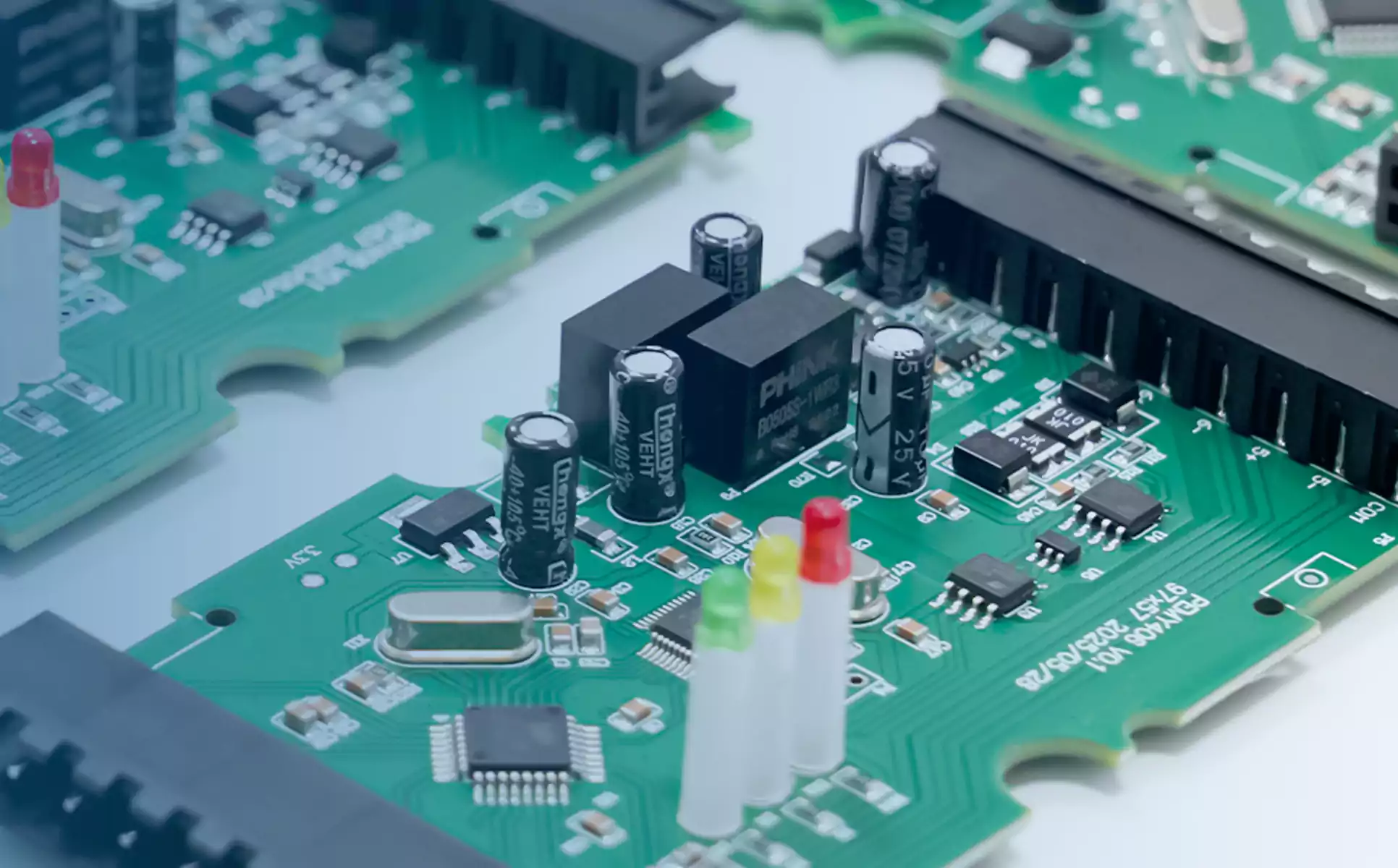
A tented via is covered by solder mask on both sides, which is adequate for a signal via but not for one inside a pad, because the mask cannot survive the soldering process. The next step up is a plugged via, where a resist is pushed into the barrel and cured, and the top of the hole is left flush enough to print on.
A fully filled and capped via is the reliable answer for thermal work. The hole is filled with a conductive or non-conductive epoxy, cured, and the surface is planarised so that the pad is genuinely flat, and in some processes it is then plated over so that the copper is continuous across the land.
Paste Escape and Stencil Aperture
Paste escape describes the path the printed paste takes when it melts, and it is the reason a filled via should sit at the centre of the pad rather than at its edge. Where a via is close to the aperture boundary, the paste flows towards the hole instead of towards the component termination.
The stencil aperture therefore has to be sized for the pad rather than for the joint alone. A slightly reduced aperture with a well defined wall, and a paste volume that leaves enough material for the fillet after some has been drawn into the hole, gives a more reliable result than a generous print that floods a partially filled via.
Thermal Pad Design for Power Devices
Under a power package the hole array is what moves the heat, and the design has to treat it as a thermal network rather than as a set of individual vias. The copper area directly under the pad, the number and diameter of the holes, and the plane they connect to all decide the junction temperature.
The far side of the board matters as well. Heat arriving on an inner plane still has to leave, and a plane that is only connected to the device and to nothing else will simply rise in temperature. Our thermal management notes describe how the copper and the holes are combined.
Voiding and Process Control
Voiding inside the joint is the most common defect, and it comes from flux trapped under the pad, from an incompletely filled hole and from a profile that does not give the volatiles time to escape. A slow ramp with a proper soak reduces it, and a paste with a low voiding characteristic helps further.
The filling process has its own controls. The epoxy must be cured to its specified schedule, the surface must be sanded or planarised without dishing the pad, and the copper plating over the cap must be thick enough to survive the assembly process without lifting. Our hole types notes describe the alternatives.
Inspection and Acceptance
Inspection has to look under the package, which means x-ray rather than optical methods. A void percentage per pad, a check that the barrel is filled, and a look at the cap for cracks or separation are the measurements that predict whether the joint will survive thermal cycling.
A coupon sectioned after assembly shows the truth: the thickness of the solder between the pad and the land, the state of the filled hole, and whether the copper cap survived. Our x-ray and AOI comparison explains when each method earns its place.
Cost and Yield Trade-Offs
Filled and capped vias cost more than tented ones, because the filling, curing and planarising steps are all additional operations with their own yield risk. On a large thermal land with many holes, that cost is usually worth paying, because a single wicking failure removes a power device.
On the rest of the board the cheapest adequate treatment is usually enough. A design that specifies filled and capped vias everywhere pays for capability it does not need, while one that tents a via inside a thermal pad takes a reliability risk for the sake of a few cents.
Working With the Fabricator
The fabrication drawing should say which vias are filled and which are only tented, and it should give the fill material, the required flatness and the plating over the cap. Leaving the distinction to be inferred from a layer image is how a good design arrives with the wrong treatment applied.
It also helps to agree the test that proves the result. A filled via that is not planarised will print badly, and a filled via that is not fully cured will outgas during reflow, so agreeing on a coupon check beforehand avoids a dispute after the panels are built. Our test coupon notes describe how that evidence is produced.
FAQ
Can a tented via be used inside a pad? It can be used for a signal pad on a low risk assembly, but not for a thermal pad or a large land. The mask over the hole usually ruptures during reflow, and the solder then wicks into the barrel.
Does filling a via make it conductive? Only if a conductive fill is specified. Non-conductive epoxy fill is common for thermal vias because the copper barrel already carries the heat, and the fill is there to stop the solder, not to conduct it.
How does gopcb handle via in pad orders? We confirm the fill and cap requirement, agree the flatness and plating specification, control the cure schedule with the job record, and provide x-ray and sectioning evidence where the customer asks for it.