Copper Pour and Via Connection Rules for PCB Layout
Copper pour is one of the last steps in a layout and one of the easiest places to introduce a defect, because the connection between the pour and every via, pad and plane is controlled by rules rather than by the router. Getting the connection style right changes yield, solderability and thermal behaviour, and the settings are rarely reviewed once the board is routed.
Why Copper Pour Needs Rule Control
A copper pour is a large area of copper that fills the empty space on a layer. It is added for return current, shielding, thermal spreading and sometimes simply to balance copper distribution before lamination. Because it touches many objects, every one of those contact points is a rule decision rather than a drawing decision.
The relevant rules live in three groups: electrical clearance, plane and polygon connections, and manufacturing constraints. A review that only checks trace spacing will pass a board whose pour connections are wrong, so the design rule set has to be examined as a whole before the layout is released.
Thermal Relief Versus Direct Connection
A thermal relief connects a pad or via to the pour through a small number of narrow spokes, which slows heat loss during soldering. A direct connection joins the copper with a full ring, which is electrically and thermally better but makes hand soldering and some reflow profiles much harder.
The usual compromise is to relief-connect pads that will be soldered and directly connect everything else. Vias that carry return current, and vias under a device that depends on the pour for heat spreading, are normally connected solidly so the copper does the job it was added for.
Setting the Polygon Connect Style
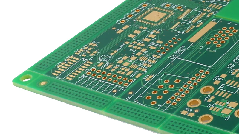
In most tools the connection style is set by a polygon connect rule that applies to a query, so a single rule can target all vias or all pads of a given type. Changing the query from relief to direct and repouring the layer is the standard way to remove the spoke pattern on vias.
The reason to do it deliberately rather than by habit is that the two styles have opposite consequences. Removing spokes lowers via inductance slightly and improves current capacity, but it also makes the via a heat sink during assembly, which matters on a thick board with a large ground area behind it.
Board Edge Pullback and Copper Clearance
Copper is normally held back from the board outline, typically by around 20 mil, to keep the edge clean after routing and to prevent exposed copper from shorting against a housing. The distance also protects the plating on the edge from mechanical damage during depanelling.
The pullback is usually implemented with a keepout or by assigning a larger clearance to the pour than to ordinary traces. Using a rule is cleaner than editing the polygon, because the pour can then be regenerated without losing the offset, as described in the standard pad design practice for edge features.

Dead Copper and Islands
Isolated fragments of copper that connect to nothing are usually removed, because they float to an undefined potential and can act as an antenna or a stray capacitance. Most tools remove islands by default, and leaving them in place is rarely a deliberate decision.
There is one case where a small island is retained, and that is when it improves copper balance on a thin core. Even then the island should be tied to a net, because a floating patch of copper on an inner layer is a reliability question rather than a cosmetic one.
Return Current and Plane Integrity
A pour is only useful as a reference if the return current can follow the signal. Splits, slots and dense via fields under a high speed trace force the return path to detour, which enlarges the loop area and radiates. Keeping the reference continuous matters more than the pour itself.
Where a power plane has to be divided, the signals crossing the boundary should be grouped and given a stitching capacitor nearby, so the return current has a defined route. Copper fill with a solid connection to vias helps here, but it cannot repair a reference plane that has been cut into unrelated pieces.
Practical Review Checklist
Check the connect style of every via, then of every pad, and confirm that the exceptions are intentional. Look at the pullback at the outline, the clearance to mounting holes and the treatment of any area where a connector shell or a metal chassis will touch the board.
Finally, repour and rerun the rule check after any change to the stackup or the outline, because these edits silently move copper. A pour that was correct before a mechanical change is not automatically correct afterwards, and the resulting shorts are found in assembly rather than in the tool.
Connection Style on Mixed-Signal Layers
On a board that carries both analogue and digital circuits, the pour under each domain should be treated separately. Analogue return current belongs in the analogue copper, and a single continuous fill that bridges the two domains gives the noise a path straight into the sensitive circuitry.
The usual solution is to keep the pour divided along the same boundary as the plane and to join the two areas at one point only. Vias in the analogue area connect directly to the analogue copper, vias in the digital area to the digital copper, and the small bridge between them is the controlled return path.
Pour Density and Manufacturing Effects
Large solid areas of copper behave differently in the press than sparse areas, so an unbalanced fill can pull a thin panel out of flat. Where the pour covers only part of a layer, the design is easier to laminate if the copper is distributed evenly rather than concentrated in one region.
Etching is affected as well. A dense fill next to fine traces produces uneven etch rates, which is why a mesh or hatched fill is sometimes chosen instead of a solid one. The choice between solid and hatched copper is a trade between electrical performance, thermal behaviour and how well the fabricator can hold the artwork dimensions.
When to Fill and When to Leave Empty
Fill the areas that carry return current, that need to spread heat, or that sit under a device with a thermal pad. Leave empty the areas where a fill would create a stub, couple noise between unrelated circuits, or interfere with an antenna keepout or an impedance-controlled structure.
The decision should be recorded in the layout notes rather than left in the tool settings, because the next engineer to open the file needs to know which fills are functional and which are simply the default. That record also prevents a later edit from silently repouring an area that was deliberately left clear.
Common Mistakes With Copper Connections
The most frequent mistake is a blanket rule that applies one connection style everywhere, so either every pad is relief connected and thermal pads under a power device stop working, or everything is direct and hand rework damages a pad. Both outcomes come from not separating the pad classes.
The second is forgetting to repour after a change. Adding a component, moving the outline or editing a keepout all alter the polygon, and the copper that is regenerated afterwards may no longer clear a feature that it previously respected. A repour followed by a full rule check closes that gap cheaply.
FAQ
Should vias be connected to copper pour with spokes? Only when a via must be soldered or when heat loss during reflow has to be limited. Return and thermal vias are normally connected directly so the copper can carry current and spread heat.
How far should copper be held back from the board edge? About 20 mil is the common figure for routed outlines. The exact value depends on the depanelling method and the housing, and it should be set as a rule rather than drawn manually.
Does a copper pour improve signal integrity by itself? Not automatically. It helps when it provides a continuous return path close to the signal. A fragmented pour with dead copper and long detours can make the return path worse than no pour at all.