What Is a Single-Sided PCB?
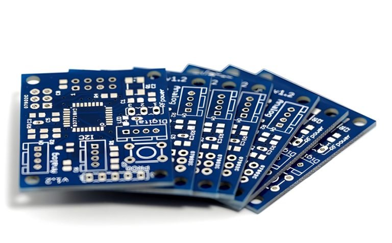
A Single-Sided PCB is a printed circuit board with a conductive copper layer on only one side of the substrate. The copper layer can be located on either the top or bottom side of the board, depending on the circuit design and assembly requirements.
Among the three primary PCB classifications based on the number of conductive layers, a Single-Layer PCB is the simplest. The other two major categories are double-sided PCBs and multilayer PCBs. Because a single-sided board uses only one copper layer, its design, manufacturing, and assembly processes are generally less complex than those of boards with multiple conductive layers.
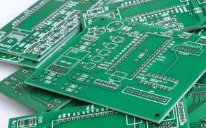
A Single-Sided PCB typically consists of a substrate, one copper layer, solder mask, surface finish, and silkscreen. Electronic components are mounted on the board, while the copper traces provide the electrical connections between components.
The simple structure of a single-sided board makes it particularly suitable for products that do not require high circuit density or complex routing. It is widely used in consumer electronics, lighting equipment, industrial controls, power supplies, automotive electronics, and other cost-sensitive applications.
Although modern electronic products increasingly use multilayer and high-density PCBs, single-sided boards remain an important PCB solution because of their low manufacturing cost, simple structure, reliable production process, and suitability for high-volume production.
Single-Sided PCB Structure
Understanding the PCB Structure is an important first step in understanding how a single-sided circuit board works and how it is manufactured.
A typical single-sided PCB consists of several functional layers and materials.
Substrate
The substrate provides the mechanical foundation of the PCB. It supports the copper layer and electronic components while maintaining the required mechanical strength and dimensional stability.
For rigid single-sided PCBs, FR-4 is one of the most commonly used substrate materials. FR-4 is a glass-fiber-reinforced epoxy laminate with good mechanical strength, electrical insulation, thermal stability, and flame-retardant properties.
Depending on the application, other substrate materials may also be used. For example, flexible single-sided PCBs can use polyimide as the substrate, allowing the circuit to bend or conform to a particular mechanical structure.
Metal-core substrates, such as aluminum-based materials, can also be selected when improved heat dissipation is required, particularly for LED lighting and power electronics.
Copper Layer
The copper layer is the primary conductive layer of a Single-Layer PCB. It contains the traces, pads, and other conductive features required to electrically connect components.
During manufacturing, a copper-clad substrate is patterned so that unwanted copper is removed while the required circuit pattern remains.
The copper thickness can be selected according to the electrical and mechanical requirements of the application. Standard copper thicknesses are suitable for many low-power circuits, while thicker copper may be required for high-current applications.
Solder Mask
The solder mask is a protective insulating coating applied over the copper circuitry, leaving selected pads and other areas exposed for soldering.
Although green is the most common solder mask color, other colors such as black, blue, red, yellow, and white are also available depending on the manufacturer’s capabilities and customer requirements.
The solder mask helps protect copper traces from oxidation, contamination, moisture, and accidental solder bridging. It also improves the reliability of the assembly process by helping control where solder is deposited.
Surface Finish
A PCB Surface Finish is applied to exposed copper areas, particularly solder pads, to protect the copper and improve solderability.
Common surface finishes include:
- HASL (Hot Air Solder Leveling)
- Lead-Free HASL
- ENIG (Electroless Nickel Immersion Gold)
- Immersion Tin
- OSP (Organic Solderability Preservative)
The appropriate surface finish depends on factors such as component type, soldering process, product life requirements, cost, and environmental conditions.
Silkscreen
The silkscreen provides identification and assembly information on the PCB. It can include component reference designators, polarity markings, logos, part numbers, test-point labels, and other manufacturing information.
A well-designed silkscreen helps operators and technicians identify components and improves assembly, inspection, maintenance, and traceability.
Advantages of Single-Sided PCBs
Low Cost
One of the most important advantages of a Single-Sided PCB is its low manufacturing cost.
Because the board contains only one conductive layer, it requires fewer materials and fewer manufacturing operations than double-sided and multilayer PCBs. The simpler construction can reduce material consumption, processing time, and production costs.
For high-volume products with relatively simple circuits, single-sided boards can provide an excellent balance between functionality and cost.
Simple Design and Manufacturing
The simple construction of a single-sided board makes PCB layout and production relatively straightforward.
Unlike multilayer boards, designers do not need to manage multiple internal signal, power, and ground layers. Routing is therefore easier for circuits with a limited number of connections.
The simpler PCB Manufacturing Process can also make production easier to control. Fewer layers mean fewer opportunities for layer-to-layer registration problems and other manufacturing defects.
Shorter Production Lead Time
Because fewer fabrication steps are required, Single-Sided PCB Manufacturing can generally be completed faster than the manufacturing of complex multilayer boards.
For standard specifications and stable production volumes, manufacturers can use automated production equipment to improve throughput and maintain consistent quality.
The actual lead time depends on board specifications, quantity, materials, surface finish, testing requirements, and production capacity.
Suitable for High-Volume Production
Single-sided PCBs are particularly suitable for applications where large quantities of relatively simple circuit boards are required.
Once the design and manufacturing parameters have been validated, automated production lines can efficiently manufacture large quantities of boards with consistent dimensions and electrical characteristics.
Easy Inspection and Maintenance
The simple structure of a single-sided board makes visual inspection and troubleshooting relatively convenient. Copper traces, component locations, and solder joints are generally easier to access than those on complex multilayer boards.
This can be beneficial for products that require frequent maintenance, repair, or replacement.
Applications of Single-Sided PCBs
The simple and economical characteristics of single-sided circuit boards make them suitable for a wide range of electronic products.
Typical PCB Applications include:
- LED lighting systems
- Calculators
- Coffee makers
- Toys
- Consumer electronics
- Power adapters
- Battery chargers
- Motor control systems
- Industrial control equipment
- Instrument panels
- Alarm systems
- Basic automation equipment
- Low-complexity power supplies
- Household appliances
Single-sided PCBs are most appropriate when the circuit does not require high component density, complex routing, controlled impedance, or extensive power and ground planes.
For more complicated designs, designers may need to move to double-sided or multilayer PCB technology.
Single-Sided PCB Manufacturing Process
The Single-Sided PCB Manufacturing process typically involves several key stages, from PCB design and material preparation to circuit pattern formation, surface treatment, and electrical testing.
The exact production sequence can vary depending on the board material, manufacturing technology, surface finish, and quality requirements.
PCB Schematic and Layout
The first stage of the PCB Manufacturing Process is circuit design.
Engineers create the schematic using electronic design automation (EDA) or CAD software. The schematic defines the electrical relationships between components.
After the schematic is completed, engineers create the PCB layout by placing components and routing copper traces on the available copper layer.
For single-sided boards, routing must be carefully planned because all conductive traces need to be formed on one side of the board. Designers should consider trace width, spacing, pad dimensions, component placement, thermal requirements, manufacturability, and electrical performance.
Design for Manufacturability (DFM) checks should also be performed before production to identify potential manufacturing issues.
Material Preparation
The appropriate copper-clad laminate is selected according to the application.
Material selection may depend on requirements such as:
- Electrical insulation
- Thermal performance
- Mechanical strength
- Flame resistance
- Operating temperature
- Copper thickness
- Environmental requirements
FR-4 is widely used for rigid boards, while polyimide and other materials can be selected for flexible applications.
Photoresist Application
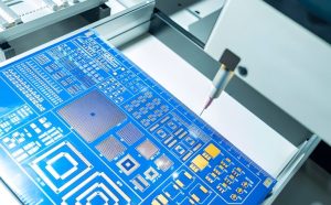
A photoresist material is applied to the copper surface. The circuit pattern is then transferred to the board using an appropriate imaging process.
The photoresist protects the areas of copper that need to remain after etching.
Modern PCB manufacturers may use automated imaging systems to improve pattern accuracy and production consistency.
Etching
During etching, unwanted copper is chemically removed from the board.
After the etching process, only the copper required for the designed circuit pattern remains.
The board is then cleaned to remove residual chemicals and contaminants. Proper control of etching parameters is essential because over-etching can reduce trace width, while under-etching can leave unwanted copper between adjacent circuits.
Drilling
Holes may be drilled according to the PCB design and component requirements.
On a basic single-sided PCB, holes can be used for through-hole component leads and mechanical requirements. Depending on the design, hole sizes and tolerances must be carefully controlled to ensure reliable component insertion and soldering.
Unlike multilayer boards, a conventional single-sided PCB does not require interconnection between multiple copper layers. Therefore, its via requirements are generally much simpler.
Solder Mask Application
A solder mask is applied to protect the copper circuitry.
The solder mask is selectively exposed and developed so that solderable pads remain open while the surrounding copper traces are protected.
After curing, the solder mask provides electrical insulation and mechanical protection for the circuit.
Surface Finishing
A suitable PCB Surface Finish is applied to exposed copper pads.
HASL is a traditional and economical surface finish, while lead-free HASL is commonly used when environmental requirements restrict lead-containing materials.
ENIG can provide a flat surface and good solderability, making it suitable for applications with tighter assembly requirements. OSP and immersion tin are also used for specific applications.
The surface finish should be selected according to component packages, soldering technology, storage requirements, reliability expectations, and cost.
Silkscreen Printing
Silkscreen markings are applied after the solder mask process.
The markings can identify components, polarity, board orientation, part numbers, logos, test points, and other useful information.
Clear and accurate silkscreen markings can reduce assembly errors and make inspection and maintenance easier.
Electrical Testing and Inspection
Testing is an essential stage of the PCB Manufacturing Process.
Depending on production requirements, manufacturers may use:
- Automated Optical Inspection (AOI)
- Flying Probe Testing
- In-Circuit Testing (ICT)
- Electrical continuity testing
- Insulation testing
- Visual inspection
For large-volume production, ICT can be useful when an appropriate test fixture is available. Flying probe testing can provide greater flexibility for prototypes and smaller production quantities because it does not require a dedicated fixture.
The testing method should be selected according to production volume, circuit complexity, quality requirements, and cost considerations.
Design Considerations for Single-Sided PCBs
Although single-sided boards are relatively simple, careful design is still required to achieve reliable manufacturing and assembly.
Trace Width and Spacing
Because all routing must be completed on a single copper layer, designers need to optimize trace width and spacing carefully.
High-current traces should be designed with sufficient width and copper thickness to handle the expected current and temperature rise.
Component Placement
Component placement should consider routing efficiency, assembly accessibility, thermal performance, and mechanical constraints.
Placing components strategically can reduce unnecessary trace crossings and improve the manufacturability of the board.
Thermal Management
Components that generate significant heat require appropriate thermal design.
Depending on the application, designers may use wider copper areas, thermal pads, heatsinks, or metal-core PCB materials to improve heat dissipation.
Manufacturing Tolerances
Designers should always consider the actual manufacturing capabilities of the PCB supplier.
Minimum trace width, spacing, hole diameter, annular ring, board thickness, copper thickness, solder mask clearance, and other parameters should be compatible with the manufacturer’s process capabilities.
Following DFM principles during the design stage can reduce production problems and improve overall yield.
Single-Sided PCB vs. Double-Sided PCB vs. Multilayer PCB
The main difference between these PCB types is the number of conductive layers and the resulting design complexity.
| PCB Type | Conductive Layers | Complexity | Cost | Typical Applications |
|---|---|---|---|---|
| Single-Sided PCB | 1 | Low | Low | Simple electronic products |
| Double-Sided PCB | 2 | Medium | Medium | More complex consumer and industrial electronics |
| Multilayer PCB | 4 or more | High | Higher | High-density and high-performance electronics |
A Single-Layer PCB is generally the best option when the circuit is simple and cost efficiency is a priority.
A double-sided PCB provides additional routing space and allows designers to use both sides of the board for conductive patterns.
Multilayer PCBs provide even greater routing density and allow dedicated power, ground, and signal layers. They are widely used in computers, networking equipment, communication systems, medical electronics, automotive electronics, and other advanced products.
Therefore, PCB layer selection should be based on electrical requirements, component density, mechanical constraints, production volume, reliability requirements, and overall cost.
Why Choose Kingda for Single-Sided PCB Manufacturing?
Choosing the right PCB manufacturer is essential for maintaining stable quality, consistent production, and competitive costs.
Kingda provides PCB manufacturing solutions for different application requirements, including standard single-sided circuit boards and more complex PCB technologies.
Our manufacturing approach focuses on process control, production consistency, inspection, and customer requirements. By combining appropriate materials, automated manufacturing equipment, quality control procedures, and experienced engineering support, Kingda helps customers achieve reliable PCB production.
Key advantages include:
- Stable and consistent PCB quality
- Competitive manufacturing costs
- Flexible production quantities
- Efficient production and delivery
- Professional engineering support
- One-stop PCB manufacturing services
- Strict quality inspection and testing
For simple, cost-sensitive, and high-volume electronic products, a Single-Sided PCB can still be an efficient and reliable solution.
Understanding the board’s PCB Structure, manufacturing requirements, material selection, and application conditions allows engineers to determine whether single-sided PCB technology is suitable for their project. When the design does not require high circuit density or complex multilayer routing, single-sided construction can provide an effective combination of simplicity, reliability, and cost efficiency.