ENIG Surface Finish PCB: Process, Advantages, Defects, Reliability, and Applications
As PCB manufacturing processes continue to evolve, manufacturers are adopting advanced techniques across individual production stages to meet increasingly complex design requirements and achieve consistent electrical, mechanical, and thermal performance. Every stage of PCB fabrication and assembly—from material selection and circuit formation to plating, surface finishing, assembly, and inspection—plays an important role in determining the reliability of the finished circuit board.
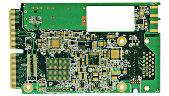
PCB materials and exposed copper surfaces are particularly vulnerable to oxidation, contamination, humidity, and other environmental factors. Without adequate protection, exposed copper can oxidize and deteriorate, affecting solderability, electrical connections, and long-term reliability. To address these challenges, manufacturers use various PCB surface finishes, including HASL, OSP, immersion tin, immersion silver, ENIG, and ENEPIG.
Among these options, ENIG surface finish has become one of the most widely adopted solutions for high-density circuit boards, fine-pitch components, BGA packages, and applications requiring a flat and reliable solderable surface.
What Is ENIG Surface Finish?
ENIG (Electroless Nickel Immersion Gold) is a two-layer metallic surface finish applied to exposed copper pads on a PCB.
The structure generally consists of:
- An electroless nickel layer deposited directly onto the exposed copper.
- A very thin immersion gold layer deposited over the nickel.
- The nickel layer acts as a barrier between copper and solder while providing mechanical support for the surface finish.
- The gold layer protects the nickel surface from oxidation and contamination before assembly.
Unlike electrolytic gold plating, immersion gold is deposited through a displacement reaction and is intentionally very thin. During soldering, most of the gold dissolves into the solder, while the nickel layer remains as the primary barrier and solderable surface.
The exact nickel and gold thicknesses should be controlled according to the applicable specification, PCB design, assembly requirements, and manufacturer process capability rather than treated as universal values.
The basic ENIG structure can be represented as:
Copper → Electroless Nickel → Immersion Gold
This combination provides excellent surface flatness, oxidation resistance, solderability, and storage stability, making ENIG particularly suitable for modern high-density PCB assembly.
How Does the ENIG Process Work?
The ENIG process involves several controlled chemical treatment and deposition steps.
1. Copper Surface Preparation
Before nickel deposition, the exposed copper pads must be thoroughly cleaned and activated. Surface contaminants, oxides, oils, and residues can interfere with deposition and reduce coating uniformity.
Proper surface preparation is essential for achieving good adhesion and consistent plating quality.
2. Electroless Nickel Deposition
A controlled electroless plating process deposits nickel onto the exposed copper surfaces without requiring an external electrical current.
The nickel layer provides several important functions:
- Acts as a diffusion barrier between copper and solder
- Protects the underlying copper
- Provides a hard and stable solderable surface
- Improves wear resistance
- Supports the subsequent immersion gold layer
Nickel bath chemistry must be carefully controlled because parameters such as temperature, pH, chemical concentration, deposition rate, and phosphorus content can affect coating characteristics and reliability.
3. Immersion Gold Deposition
After nickel deposition, the exposed nickel surface undergoes an immersion gold process.
Gold is deposited through a controlled displacement reaction in which a thin layer of gold replaces a small amount of surface nickel. Because the immersion reaction is self-limiting, the resulting gold layer is much thinner than conventional plated gold.
The gold layer primarily protects the nickel from oxidation and contamination before soldering.
4. Cleaning and Inspection
After plating, the PCB undergoes rinsing, drying, and inspection.
Manufacturers may inspect:
- Nickel and gold coating thickness
- Surface uniformity
- Pad appearance
- Plating adhesion
- Corrosion or discoloration
- Solderability
- Surface contamination
Advanced PCB inspection methods can help identify plating defects before the boards enter the assembly process.
Why Is ENIG Important for PCB Assembly?
One of the biggest advantages of ENIG is its ability to provide a flat, uniform surface for component assembly.
Modern electronic products increasingly use:
- Fine-pitch ICs
- BGA packages
- QFN packages
- Micro-BGA components
- Small passive components
- High-density interconnects
- Advanced surface-mount technology
These components require accurate pad geometry and consistent solder deposition. ENIG provides a relatively flat surface compared with traditional HASL, making it well suited to fine-pitch SMT assembly.
The surface finish also helps protect exposed copper during PCB storage and handling, provided that the boards are manufactured, packaged, and stored correctly.
Long-Term Reliability of ENIG Solder Joints
A properly manufactured ENIG PCB can provide excellent long-term solder-joint reliability across demanding operating environments.
This makes ENIG suitable for applications such as:
- Automotive electronics
- Industrial control systems
- Telecommunications equipment
- Medical electronics
- Aerospace electronics
- Defense systems
- High-density computing equipment
- Consumer electronics
The nickel layer acts as a barrier that limits copper dissolution into the solder joint. Meanwhile, the gold layer protects the nickel surface before assembly.
For demanding applications, reliability depends not only on the surface finish but also on PCB laminate selection, copper thickness, pad design, solder alloy, reflow profile, component selection, assembly quality, and environmental conditions.
Therefore, ENIG should be considered as part of the complete PCB manufacturing and assembly reliability strategy rather than as an isolated reliability solution.
ENIG vs. Other PCB Surface Finishes
Choosing the appropriate PCB surface finish depends on component pitch, assembly process, cost, storage requirements, reliability targets, and application environment.
ENIG vs. HASL
HASL is generally more economical than ENIG and has long been used for conventional PCB applications. However, the solder coating created by HASL is less planar than ENIG.
ENIG offers several advantages for:
- Fine-pitch components
- BGA packages
- QFN packages
- High-density PCB layouts
- Applications requiring consistent pad flatness
Lead-free HASL can provide good performance but typically involves higher processing temperatures and may introduce greater surface-height variation than ENIG.
ENIG vs. OSP
OSP uses an organic protective coating to protect exposed copper surfaces.
Its main advantages include low cost and a relatively flat surface. However, OSP is more sensitive to handling and storage conditions because the protective organic layer can be damaged or degraded.
ENIG generally offers better surface durability and longer storage stability, making it attractive for applications involving more demanding handling or longer manufacturing cycles.
ENIG vs. ENEPIG
ENEPIG (Electroless Nickel Electroless Palladium Immersion Gold) adds a palladium layer between nickel and gold.
Its advantages can include excellent solderability, wire-bonding capability, and improved resistance to certain nickel corrosion mechanisms associated with immersion-gold processing.
However, ENEPIG generally has a higher process cost than ENIG.
For many applications that primarily require reliable soldering and a flat surface, ENIG provides a strong balance between performance and manufacturing cost.
ENIG vs. Immersion Silver and Immersion Tin
Immersion silver and immersion tin can provide good solderability and relatively flat surfaces.
However, their surface stability can be affected by environmental exposure, contamination, oxidation, or improper storage. Their suitability therefore depends heavily on application requirements and storage conditions.
ENIG generally provides a more robust combination of surface protection, flatness, solderability, and storage stability for many high-density applications.
| Surface Finish | Flatness | Cost | Storage Stability | Fine-Pitch Suitability | Typical Applications |
|---|---|---|---|---|---|
| ENIG | Excellent | Medium–High | Excellent | Excellent | BGA, fine-pitch, industrial, automotive |
| HASL | Moderate | Low | Good | Moderate | General-purpose PCBs |
| OSP | Excellent | Low | Moderate | Good | Cost-sensitive SMT applications |
| ENEPIG | Excellent | High | Excellent | Excellent | High-reliability and wire bonding |
| Immersion Silver | Excellent | Medium | Moderate | Good | High-density electronics |
| Immersion Tin | Excellent | Medium | Moderate | Good | General SMT applications |
The best finish depends on the specific PCB design, assembly technology, reliability requirements, and manufacturing environment.
Common ENIG PCB Defects
Although ENIG offers many advantages, improper process control can lead to plating and solderability problems.
Black Pad and Nickel Corrosion
The so-called black pad phenomenon is one of the best-known reliability concerns associated with ENIG.
It is generally related to excessive or localized corrosion of the nickel surface during the immersion-gold process. Depending on the severity and mechanism, the affected surface may appear dark or discolored and may exhibit poor solderability.
Factors that can contribute to nickel corrosion include:
- Poorly controlled immersion-gold chemistry
- Excessive immersion activity
- Improper bath conditions
- Nickel surface characteristics
- Inadequate process control
- Contamination
The problem can reduce solder-joint reliability and may be difficult to detect through visual inspection alone.
A well-controlled ENIG process, regular chemical-bath monitoring, and appropriate quality testing are therefore essential.
Nickel Layer Defects
Other nickel-related problems can include:
- Uneven nickel deposition
- Pinholes
- Surface contamination
- Incomplete plating
- Poor adhesion
- Excessive surface roughness
- Localized corrosion
These defects can interfere with solder wetting and may contribute to unreliable electrical or mechanical connections.
Gold Embrittlement
Gold embrittlement occurs when excessive gold remains in a solder joint and contributes to the formation of brittle gold-containing intermetallic phases.
Because immersion gold is intentionally very thin, properly controlled ENIG processes significantly reduce this risk. The gold thickness should nevertheless be maintained within the applicable specification.
The objective is to provide sufficient protection for the nickel while avoiding unnecessary gold thickness that could adversely affect solder-joint reliability.
Storage and Handling Problems
Although ENIG generally provides good storage stability, improper handling and storage can still reduce solderability.
Potential risks include:
- High humidity
- Sulfur-containing contaminants
- Dust and chemical contamination
- Excessive temperature
- Direct contact with PCB pads
- Damaged packaging
- Prolonged exposure to uncontrolled environments
Manufacturers should follow the PCB supplier’s recommended storage conditions and moisture-control procedures.
Best Practices for Improving ENIG Solderability
Achieving consistent ENIG performance requires strict control throughout both PCB manufacturing and PCB assembly.
Control the ENIG Chemical Process
The plating chemistry should be monitored continuously or at defined intervals according to the manufacturer’s process-control system.
Important parameters may include:
- Bath temperature
- pH
- Chemical concentration
- Nickel deposition rate
- Phosphorus content
- Immersion-gold chemistry
- Processing time
- Contamination levels
Consistent chemical control helps prevent excessive nickel corrosion and uneven deposition.
Maintain Appropriate Coating Thickness
Nickel and gold thickness should be selected and controlled according to the applicable specification and application requirements.
The gold layer should be thick enough to protect the nickel during storage and handling but not unnecessarily thick for a solderable surface.
Optimize the Reflow Profile
During PCB assembly, the reflow profile should be optimized for the selected solder alloy and component package.
Avoid unnecessarily high temperatures or excessive time above liquidus because inappropriate thermal profiles can accelerate intermetallic growth and increase thermal stress.
The correct profile should be established through thermal profiling and verified against the solder paste and component manufacturer’s recommendations.
Improve PCB Handling
Operators should avoid unnecessary contact with exposed pads.
Proper handling procedures include:
- Using clean gloves
- Avoiding direct contact with pads
- Keeping boards in protective packaging
- Controlling humidity
- Preventing exposure to contaminants
- Following appropriate storage-life requirements
Perform Solderability and Reliability Testing
For demanding applications, manufacturers can use appropriate testing methods to verify surface-finish quality and assembly reliability.
Depending on the application, testing may include:
- Solderability testing
- Microsection analysis
- Coating-thickness measurement
- Surface inspection
- Cross-sectional analysis
- Thermal cycling
- Environmental testing
- Electrical testing
Combining process monitoring with laboratory and production-line inspection provides greater confidence in long-term PCB reliability.
ENIG PCB Applications
ENIG is widely used across industries where flat pads, reliable solderability, and good surface protection are important.
Automotive Electronics
Automotive control units, sensors, infotainment systems, battery-management electronics, and advanced driver-assistance systems often use high-density PCBs with fine-pitch components.
ENIG can provide a suitable surface for these assemblies when the complete PCB design and manufacturing process meets the required reliability standards.
Industrial Electronics
Industrial controllers, power-management systems, instrumentation, automation equipment, and communication systems can benefit from ENIG’s flat surface and good storage stability.
Aerospace and Defense
Aerospace and defense electronics often require strict process control, traceability, inspection, and reliability verification.
ENIG may be selected for high-density assemblies where consistent pad geometry and solderability are important.
Medical Electronics
Medical equipment frequently combines high-density electronics with demanding reliability requirements. ENIG can be used for control boards, diagnostic systems, monitoring equipment, and other electronic assemblies when the finish meets the relevant product requirements.
Telecommunications and Computing
High-speed communication equipment, networking devices, servers, and computing hardware often contain fine-pitch and BGA components. The planar surface provided by ENIG makes it suitable for these high-density PCB designs.
How to Choose an ENIG PCB Manufacturer
Selecting the right PCB manufacturer is essential because ENIG performance depends heavily on process control.
When evaluating a supplier, consider the following factors:
1. ENIG Process Control
The manufacturer should have a controlled plating process and appropriate monitoring procedures for nickel and gold deposition.
2. Surface-Finish Inspection
The supplier should have appropriate inspection and testing capabilities to verify coating quality, surface uniformity, solderability, and other critical characteristics.
3. Fine-Pitch PCB Capability
If the board uses BGA, QFN, micro-BGA, or other fine-pitch packages, confirm that the manufacturer can maintain the required pad geometry and surface flatness.
4. PCB Assembly Capability
If both fabrication and assembly are required, an integrated PCB assembly partner can simplify process coordination and reduce communication between separate suppliers.
5. Quality Management
A reliable manufacturer should maintain documented process controls, traceability, inspection procedures, and quality-management systems appropriate to the customer’s application.
Kingda ENIG PCB Manufacturing Support
Kingda can support customers requiring ENIG-finished PCBs for a wide range of electronic applications.
By integrating PCB fabrication, surface-finish control, inspection, and assembly requirements, Kingda can help customers develop a more consistent manufacturing process from PCB design through production.
For high-density and fine-pitch applications, the ENIG process can be coordinated with appropriate PCB stackup design, pad geometry, solder mask requirements, SMT assembly, and quality inspection.
Customers should provide their required PCB specifications, surface-finish requirements, component package information, assembly process, and reliability targets so that the manufacturing process can be matched to the final application.
Conclusion
ENIG surface finish has become one of the most widely used surface-finishing technologies for modern high-density PCBs. Its combination of a protective gold layer and electroless nickel barrier provides excellent surface flatness, oxidation protection, solderability, and storage stability.
Compared with HASL, OSP, immersion tin, immersion silver, and ENEPIG, ENIG offers a particularly strong balance of performance and cost for many fine-pitch and high-density PCB applications.
However, ENIG reliability depends heavily on process control. Nickel corrosion, black pad defects, coating irregularities, excessive gold, contamination, and improper storage can negatively affect solderability and long-term reliability.
For this reason, choosing an experienced PCB manufacturing partner with controlled ENIG chemistry, appropriate inspection capabilities, and strong process management is essential.
As electronic products continue to become smaller, denser, and more sophisticated, ENIG remains an important PCB surface finish for BGA, fine-pitch SMT, automotive electronics, industrial systems, telecommunications, medical equipment, and other high-reliability applications.