5G Base Station PCB RF Unit PCB Selection Guide: Materials, Copper Thickness, Thermal Management & Reliabilitye
The RF unit of a 5G base station performs critical functions such as signal transmission, reception, filtering, and power amplification. Unlike many conventional electronic applications, these systems must handle high-frequency signals, significant power density, heat generation, electromagnetic interference, and demanding outdoor operating conditions.
As the physical platform that carries RF components and provides electrical connections between them, the PCB has a direct influence on signal integrity, thermal performance, mechanical stability, and long-term reliability.
Selecting a suitable 5G Base Station PCB therefore requires more than simply choosing the right number of layers or board thickness. Engineers should evaluate the PCB material, copper structure, solder mask, thermal design, impedance requirements, and reliability testing as an integrated system.
This guide explains five key considerations when selecting an RF PCB for 5G base station applications.
1. Select High-Frequency Materials for Stable RF Performance
Material selection is one of the most important factors in designing a High Frequency PCB for 5G equipment.
Traditional FR-4 materials can be economical and suitable for many general-purpose applications. However, as signal frequencies increase, dielectric properties and transmission losses become increasingly important. Depending on the design frequency, signal path, and performance requirements, specialized high-frequency or hybrid materials may be more appropriate.
Key material characteristics to evaluate include:
- Dielectric constant (Dk)
- Dissipation factor (Df)
- Dielectric loss
- Dk consistency across the operating frequency range
- Thermal stability
- Coefficient of thermal expansion (CTE)
- Moisture resistance
- Dimensional stability
A stable dielectric constant helps maintain predictable transmission-line characteristics and impedance. Low dielectric loss can also reduce signal attenuation, which becomes increasingly important in high-speed and high-frequency RF applications.
Material selection should also consider the operating environment. Outdoor base stations may experience substantial temperature changes and humidity fluctuations. A material with suitable thermal and dimensional stability can help reduce the risk of warpage, delamination, and other reliability problems.
For projects requiring controlled material selection and manufacturing processes, it is important to work with a PCB manufacturer capable of handling different laminate systems and high-frequency requirements.
2. Choose Copper Thickness According to RF and Power Requirements

Copper thickness has a direct relationship with current-carrying capability, thermal performance, impedance control, and manufacturing requirements.
A 5G RF unit may contain both sensitive high-frequency signal paths and relatively high-current power sections. These different areas do not necessarily require the same copper configuration.
For RF signal routing, excessive copper thickness can affect transmission-line geometry and manufacturing tolerances. At high frequencies, conductor surface characteristics and skin-effect-related losses also become relevant.
For power amplifier and power distribution areas, however, adequate copper thickness can improve current-carrying capability and help distribute heat.
The appropriate approach is therefore to evaluate copper thickness according to the function of each circuit area rather than selecting a single value based only on current capacity.
Important considerations include:
- Required current capacity
- Characteristic impedance
- Signal frequency
- Trace width and spacing
- Thermal requirements
- Layer stack-up
- Manufacturing tolerances
- Copper-to-laminate adhesion
Copper adhesion is particularly important for equipment that experiences repeated thermal cycling. Differences in thermal expansion between copper and the dielectric material can place mechanical stress on interconnections over time.
For more demanding RF designs, the PCB stack-up should be developed together with the impedance requirements and manufacturing capabilities rather than treating copper thickness as an isolated parameter.
3. Evaluate Solder Mask for RF, Protection, and Environmental Durability
Solder mask primarily protects exposed copper from oxidation, contamination, and accidental electrical contact. However, in high-frequency applications, its electrical properties can also influence certain RF structures.
When solder mask overlaps or is positioned close to controlled-impedance RF traces, its dielectric characteristics may need to be considered during design and simulation. Depending on the RF structure, designers may specify different solder-mask configurations to maintain the required electrical performance.
A suitable solder mask should also provide:
- Good insulation performance
- Strong adhesion
- Thermal resistance
- Moisture resistance
- Resistance to environmental exposure
- Consistent coating thickness
- Good surface quality
Outdoor 5G equipment may be exposed to temperature changes, humidity, dust, and other environmental factors. A durable solder mask helps protect copper features throughout the service life of the equipment.
Surface flatness can also be important when the PCB includes fine-pitch components, RF modules, connectors, filters, or other precision components. Consistent solder-mask processing supports reliable assembly and reduces potential soldering problems.
4. Match PCB Construction With Thermal Management Requirements
Thermal management is another critical consideration when selecting a RF Circuit Board for 5G infrastructure.
RF power amplifiers and other high-power components can generate substantial heat. If this heat is concentrated around individual components, excessive junction or board temperatures can reduce component performance and accelerate aging.
PCB thermal design can incorporate several approaches, including:
Thermal Vias
Thermal vias can transfer heat from component pads or thermal regions into internal copper layers and, where appropriate, toward a heat-spreading structure.
Large Copper Areas
Copper planes can help distribute heat over a larger area while also providing electrical grounding or power distribution.
High-Thermal-Conductivity Materials
For specific applications, materials or PCB structures with improved thermal conductivity may be considered. The best solution depends on the power density, mechanical structure, heat sink arrangement, and electrical requirements.
Copper Thickness and Layer Stack-Up
Additional copper or strategically designed internal copper planes can improve heat spreading in suitable areas. However, increasing copper thickness should always be evaluated together with impedance, manufacturability, weight, and cost.
Mechanical Integration
PCB thickness and dimensions should match the enclosure, heat sink, RF shielding, connectors, and mounting structure. A PCB with excellent electrical characteristics may still be unsuitable if its physical structure conflicts with the system’s thermal or mechanical design.
For complex products, thermal management should therefore be considered during PCB design rather than added after the board layout is completed.
5. Verify Reliability Before Selecting a 5G PCB Supplier
5G base stations are typically expected to operate reliably for extended periods, often in locations where maintenance can be difficult or expensive. PCB reliability should therefore be evaluated as carefully as electrical performance.
A reliable 5G PCB should be manufactured under controlled processes and verified according to the application’s requirements.
Environmental Reliability
Depending on the deployment environment, relevant evaluations may include:
- High-temperature and humidity testing
- Temperature cycling
- Thermal shock
- Vibration testing
- Mechanical testing
- Corrosion or salt-spray testing where applicable
These tests help determine whether the PCB can maintain its mechanical and electrical integrity under environmental stress.
Electrical Testing
Electrical verification may include:
- Continuity testing
- Insulation resistance testing
- Dielectric withstand testing
- Impedance testing
- Open and short circuit inspection
The exact test requirements should be defined according to the PCB design and end-product specifications.
Manufacturing Reliability
Manufacturing quality is equally important. Engineers should pay attention to:
- Interlayer bonding
- Via reliability
- Plating quality
- Copper adhesion
- Solderability
- Dimensional stability
- Surface finish consistency
A capable supplier should be able to provide appropriate process controls and inspection records when required.
6. Key Factors at a Glance
| Selection Factor | Main Concern | What to Evaluate |
|---|---|---|
| PCB Material | RF signal performance | Dk, Df, loss, thermal stability |
| Copper Thickness | Current and RF performance | Current capacity, impedance, thermal requirements |
| Solder Mask | Protection and RF compatibility | Electrical properties, adhesion, environmental resistance |
| Thermal Design | Heat dissipation | Thermal vias, copper planes, materials, heat-sink integration |
| Reliability | Long-term operation | Environmental, electrical, and manufacturing tests |
The best 5G Base Station PCB is not necessarily the one with the most advanced material or thickest copper. It is the board whose electrical, thermal, mechanical, and environmental characteristics are properly matched to the actual system requirements.
7. Why Impedance Control Matters in 5G RF PCB Design
Impedance control deserves special attention in high-frequency applications.
RF transmission lines are designed to maintain predictable electrical characteristics between the source, transmission path, and receiving device. Variations in trace width, dielectric thickness, copper thickness, material properties, or layer registration can affect the resulting impedance.
For this reason, controlled-impedance PCB manufacturing should begin with a clearly defined stack-up.
Engineers and manufacturers should coordinate on:
- Target impedance
- Reference plane configuration
- Dielectric thickness
- Trace width
- Copper thickness
- Material Dk
- Manufacturing tolerances
- Test and verification methods
This coordination is especially important when working with multilayer RF boards, where small changes in stack-up dimensions can affect transmission-line characteristics.
8. Consider PCB Assembly Requirements Along With Fabrication
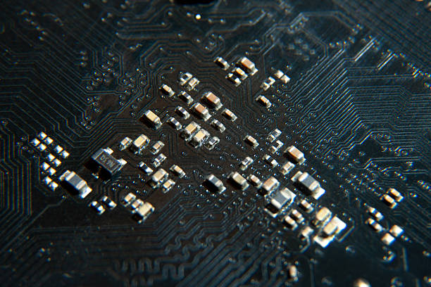
Selecting the PCB itself is only one part of the manufacturing process. RF modules often contain fine-pitch ICs, connectors, filters, power devices, shielding structures, and other components requiring precise assembly.
A supplier capable of supporting both PCB fabrication and assembly can simplify project management and reduce coordination between multiple vendors.
For prototype and engineering validation projects, Prototype PCB Assembly can help teams verify PCB design, component placement, soldering quality, and overall assembly performance before moving into larger production.
For production programs with varying volumes, Low-Volume PCB Assembly can provide greater flexibility during product introduction and early-stage manufacturing.
9. How to Choose the Right PCB Supplier for 5G RF Applications
When evaluating a PCB supplier for a 5G RF project, procurement teams should look beyond quoted price.
A practical supplier evaluation should include:
- Material capability – Can the supplier manufacture the required high-frequency or hybrid material stack-up?
- Impedance control – Can the manufacturer consistently meet the specified impedance requirements?
- Manufacturing capability – Can the supplier handle the required layer count, line/space, via structures, copper thickness, and board dimensions?
- Thermal solutions – Can the manufacturer support thermal vias, heavy copper, or other required structures?
- Quality control – Are appropriate electrical, dimensional, and visual inspections available?
- Prototype support – Can engineering samples be produced quickly enough for design validation?
- Production scalability – Can the supplier support the project when it moves from prototypes to production?
A supplier that understands both RF performance and manufacturing constraints can help identify potential problems before they become costly production issues.
10. Final Checklist for 5G Base Station RF PCB Selection
Before placing an order, confirm the following:
- PCB material is suitable for the operating frequency.
- Dk and Df requirements are clearly defined.
- Controlled impedance requirements are documented.
- Copper thickness matches both RF and power requirements.
- Thermal management has been incorporated into the PCB structure.
- Solder mask is compatible with the intended application.
- PCB dimensions and thickness match the mechanical assembly.
- Appropriate reliability testing has been defined.
- Electrical testing requirements are clear.
- The supplier has the required RF PCB manufacturing capabilities.
- Prototype and production requirements can be supported.
Conclusion
Selecting a PCB for a 5G base station RF unit requires a system-level approach. High-frequency signal performance, power handling, thermal management, environmental durability, and manufacturing reliability all need to work together.
The five most important areas are material selection, copper thickness, solder mask, thermal design, and reliability verification. Engineers should also consider controlled impedance, stack-up design, assembly requirements, and supplier manufacturing capabilities before making the final decision.
By evaluating these factors early in the design and procurement process, manufacturers can reduce RF performance risks, improve product reliability, and establish a more stable path from prototype development to volume production.
For projects requiring PCB fabrication and assembly support, provides PCB manufacturing and assembly solutions for prototype and production requirements.