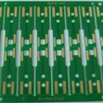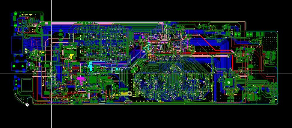
Routing is one of the most important stages in PCB Design and plays a critical role in determining the electrical performance, reliability, and manufacturability of the final product. The quality of PCB Routing can directly affect the performance of the entire electronic system, particularly in high-speed and high-frequency applications.
Compared with conventional circuit-board design, High-Speed PCB routing has much stricter requirements. Engineers must consider signal integrity, power integrity, electromagnetic interference, return-current paths, trace impedance, crosstalk, and manufacturing limitations during the routing process.
PCB routing can generally be divided into single-sided, double-sided, and multilayer routing. As PCB structures become increasingly complex, multilayer boards are now widely used to provide sufficient routing space and improve electrical performance.
At Kingda, we recommend considering the following practical routing guidelines when developing a PCB layout.
1. Avoid Parallel Routing Between Input and Output Traces
Input and output traces should generally avoid running adjacent and parallel to each other for long distances. Parallel routing can increase capacitive and inductive coupling and may result in unwanted signal interference or reflection.
Where necessary, a ground trace or grounded copper area can be placed between sensitive signal paths to provide additional isolation.
For multilayer PCBs, routing directions on adjacent signal layers can also be arranged perpendicular to each other where practical. This approach helps reduce parasitic coupling between neighboring traces.
2. Give Priority to Ground and Power Routing
In many PCB designs, the routing priority can generally be considered in the following order:
Ground → Power → Signal
Signal traces may use relatively narrow widths where appropriate, while power and ground conductors are typically designed wider to reduce resistance and voltage drop.
For digital PCBs, a solid Ground Plane is often preferred because it provides a low-impedance return path for high-speed signals and can help improve Signal Integrity.
However, grounding strategies for analog circuits should be carefully designed according to the system architecture. Simply applying the same grounding method to both analog and digital circuits may introduce unwanted noise.
3. Use Copper Pour Appropriately
Unused areas of a PCB can sometimes be filled with copper and connected to the ground network.
Ground copper pours can reduce the impedance of the return-current path, improve thermal dissipation, and help reduce electromagnetic interference.
However, copper areas should not be added without considering current flow, isolation requirements, thermal effects, and manufacturing rules.
For high-speed circuits, engineers should also make sure that copper pours do not unintentionally change the impedance of controlled-impedance traces.
4. Properly Manage Analog and Digital Ground
In mixed-signal PCB designs, analog and digital ground structures may be separated in certain applications to reduce noise coupling.
However, the actual grounding strategy should be determined according to the circuit architecture rather than simply separating the two grounds everywhere.
When analog and digital ground areas need to be connected, they should generally have a carefully controlled connection point or return-current path.
The connection between the PCB and external equipment, such as connectors, also needs to be considered because external cables can introduce noise and unwanted ground-current paths.
5. Use Power and Ground Planes Efficiently
When there is insufficient routing space on the signal layers, engineers may consider using dedicated power or ground layers within a multilayer PCB.
A well-designed Power Plane and ground plane can provide low-impedance power distribution and stable return-current paths.
In high-speed designs, power and ground planes should be positioned carefully in the stack-up to minimize loop area and reduce electromagnetic radiation.
6. Establish an Appropriate PCB Grid
Many standard electronic components use standardized pin spacing, such as 2.54 mm (100 mil).
Therefore, an appropriate design grid can simplify component placement and routing.
Common PCB layout grids include 100 mil, 50 mil, 25 mil, and smaller increments depending on component density and routing requirements.
For general placement, a 50-mil grid may be suitable for many applications, while a finer grid can be used for dense layouts and fine-pitch components.
The final grid should be selected according to the actual component package, PCB manufacturing capability, and design requirements.
7. Use Serpentine Routing Carefully
Serpentine traces are primarily used for length matching rather than simply making the routing look more organized.
They are commonly used for high-speed interfaces where multiple signal traces need to maintain similar propagation delays.
However, excessive serpentine routing can introduce additional coupling between adjacent segments and may negatively affect signal integrity.
Therefore, meander structures should be designed with appropriate spacing and should only be used when required for timing or length matching.
8. Keep Copper Away From the PCB Edge
Copper traces and copper pours should maintain an appropriate clearance from the PCB edge.
As a general design reference, a clearance of approximately 20 mil may be used where the manufacturing process permits it.
The actual edge clearance should be determined according to the PCB manufacturer’s capabilities, mechanical requirements, board outline, and electrical safety requirements.
Adequate edge clearance helps prevent accidental exposure of copper and reduces the risk of mechanical damage during PCB manufacturing and assembly.
9. Consider PCB Signal Propagation Delay
Signal propagation delay on a PCB depends on the dielectric material, trace geometry, layer structure, and signal propagation environment.
As a general reference, a PCB trace may have a propagation delay of approximately 0.167 ns/in under certain material and structural conditions.
However, the actual delay can vary significantly depending on the PCB stack-up and routing structure.
Vias, component pins, connectors, package structures, and other discontinuities can also introduce additional delay and impedance discontinuities.
For high-speed interfaces, propagation delay should therefore be evaluated as part of the overall Signal Integrity analysis.
10. Understand the Relationship Between Trace Geometry and Impedance
The characteristic impedance of a PCB trace is influenced by several factors, including:
- Trace width
- Copper thickness
- Dielectric thickness
- Distance to the reference plane
- Dielectric constant
- Trace geometry
In general, increasing trace width tends to reduce characteristic impedance, while increasing the distance between the trace and its reference plane tends to increase impedance.
The dielectric constant of the PCB material also affects the propagation characteristics and impedance.
For applications requiring Controlled Impedance, the trace width and layer structure should therefore be calculated based on the selected PCB material and stack-up.
11. Treat PCB Traces as Distributed Electrical Structures
At high frequencies, PCB traces cannot always be treated as simple wires.
Depending on the signal frequency and electrical length, a trace may exhibit distributed resistance, capacitance, and inductance.
For high-speed designs, engineers should consider:
- Trace resistance
- Trace inductance
- Parasitic capacitance
- Return-current paths
- Characteristic impedance
- Signal reflection
These parameters can affect signal rise time, overshoot, ringing, crosstalk, and overall signal quality.
Therefore, high-speed PCB routing should be evaluated based on transmission-line behavior rather than simply the physical connection between two points.
12. Keep High-Speed Interconnects Short
For relatively low-speed CMOS or TTL circuits, PCB trace length may not always be a critical design factor.
However, as signal rise time becomes faster, even circuits with a relatively low clock frequency can exhibit transmission-line effects.
Instead of relying only on operating frequency, engineers should consider signal rise time, propagation delay, and electrical length when determining whether a trace should be treated as a high-speed interconnect.
For fast signals, shorter routing paths are generally preferred, and unnecessary vias, bends, connectors, and other discontinuities should be minimized.
13. Keep High-Power Components Close Together
High-power components and their associated power-distribution components should generally be placed close to each other where practical.
Shorter power paths help reduce parasitic inductance and resistance and can minimize transient voltage overshoot.
Decoupling capacitors should also be positioned close to the power pins of the corresponding ICs.
This placement strategy can improve power integrity and reduce high-frequency noise.
14. Understand Layer Switching During PCB Routing
When routing multilayer PCBs, changing signal layers generally requires vias to establish an electrical connection between the different layers.
The routing behavior depends on the PCB design software and the routing mode being used.
Engineers should therefore understand how the selected PCB design software handles layer changes, via insertion, routing rules, and design-rule checking.
After routing is completed, all vias and layer transitions should be reviewed to ensure that they comply with the PCB stack-up and manufacturing requirements.

15. Set the Appropriate Trace Width Before Routing
In PCB design software, trace width can generally be configured before starting a routing operation.
After selecting the starting point of a trace, the current routing width is displayed in the software interface. The width can then be adjusted according to the electrical requirements of the specific net.
Different signal types may require different trace widths.
For example, power traces may require wider conductors to carry higher current, while high-speed controlled-impedance traces must use a specific width based on the PCB stack-up and target impedance.
Therefore, trace width should not be selected solely according to physical space. It should also consider current capacity, impedance requirements, temperature rise, manufacturing tolerances, and signal integrity.
Conclusion
Good PCB Routing is essential for achieving reliable electrical performance, particularly in high-speed and high-density electronic products.
A well-designed PCB layout should consider not only whether all components are electrically connected, but also how signals, power, and return currents move through the board.
Key factors such as Signal Integrity, Ground Plane design, Power Plane configuration, controlled impedance, trace length, layer transitions, component placement, and manufacturing tolerances should be considered from the beginning of the PCB Design process.
As PCB technology continues to develop toward higher density and faster signal transmission, traditional routing methods alone may no longer be sufficient for demanding applications.
Kingda recommends combining appropriate PCB materials, stack-up design, routing rules, simulation, and manufacturing capabilities to achieve a balance between electrical performance, reliability, and production efficiency.
Through careful layout planning and professional PCB Routing practices, engineers can reduce signal interference, minimize manufacturing risks, improve product reliability, and create PCB designs that are better suited for modern high-speed electronic applications.