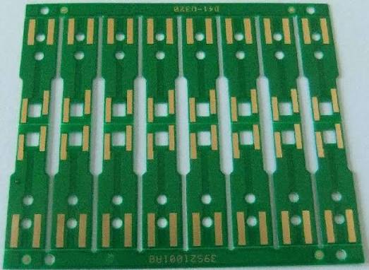
The development of PCB technology is closely connected with advances in electronic technology. As electronic products continue to evolve toward higher integration, smaller form factors, faster signal transmission, and greater functional density, conventional PCB manufacturing processes are facing increasingly demanding technical requirements.
Traditional PCB Manufacturing primarily relies on subtractive processing, commonly known as the copper etching process. In this method, a copper-clad insulating substrate is processed using a chemical etching solution to remove unwanted copper and retain the required conductive patterns.
For double-sided and multilayer circuit boards, electrical connections between different layers are established through drilled holes, plated through-holes, blind vias, and buried vias.
Although the traditional subtractive process remains widely used, it becomes more challenging when manufacturing extremely fine circuits and high-density interconnect structures. In particular, modern HDI PCB applications require finer line widths and spacing, smaller microvias, higher registration accuracy, and more precise process control.
At the same time, manufacturers are under increasing pressure to improve production efficiency, reduce material consumption, control manufacturing costs, and develop more environmentally responsible processes.
For this reason, continuous technological improvement is essential for the future development of PCB manufacturing.
Multilayer PCB and Interlayer Interconnection Technology
A Multilayer PCB uses multiple conductive layers separated by dielectric materials. Electrical connections between different layers can be achieved through plated through-holes, blind vias, and buried vias.
Compared with conventional two-layer boards, multilayer PCBs provide significantly greater routing capacity within a limited board area.
Four-layer PCBs are commonly used in many electronic products, while six-layer, eight-layer, ten-layer, and even higher-layer-count boards are also widely used in applications requiring higher circuit density and improved power and signal integrity.
The number of PCB layers cannot always be determined simply by looking at visible vias because different via structures may be used depending on the board design. Through-hole vias generally extend through the entire PCB, while blind and buried vias may connect only selected layers.
Therefore, accurate identification of PCB layer count should be based on the actual board structure, manufacturing documentation, cross-sectional analysis, or other appropriate inspection methods rather than visual inspection alone.
High-Precision and High-Frequency PCBs
The development of High-Frequency PCB technology places greater emphasis on material selection, dielectric performance, dimensional stability, surface characteristics, and transmission-line design.
A typical Copper-Clad Laminate (CCL) is manufactured using copper foil, reinforcement materials, and resin systems.
Reinforcement materials may include glass fabric, glass mat, or paper-based materials. These materials are impregnated with resin and partially cured to form prepreg. The prepreg is then combined with copper foil and laminated under controlled temperature and pressure to produce the required copper-clad laminate.
The selection of laminate materials has a direct influence on the electrical, thermal, mechanical, and manufacturing characteristics of the finished PCB.
For high-frequency and high-speed applications, engineers must consider properties such as:
- Dielectric constant (Dk)
- Dissipation factor (Df)
- Thermal stability
- Dimensional stability
- Copper surface roughness
- Moisture resistance
- Resin content
- Glass transition temperature (Tg)
- Coefficient of thermal expansion (CTE)
Proper control of these properties is particularly important for high-speed signal transmission.
Classification of Copper-Clad Laminates
Copper-Clad Laminate (CCL) generally consists of three major components: copper foil, reinforcement material, and resin.
CCLs can be classified according to their reinforcement materials, resin systems, electrical properties, thermal characteristics, and intended applications.
Classification by Reinforcement Material
Common reinforcement materials include glass fabric, glass mat, and various paper-based materials.
Based on the reinforcement type, CCLs can generally be divided into glass-fabric-based laminates and paper-based laminates.
Glass-fabric-based materials are widely used in high-performance rigid PCBs because they provide good mechanical strength and dimensional stability.
Classification by Resin System
Different resin systems can be used depending on the required electrical, thermal, and mechanical properties.
Common resin systems include:
- Epoxy resin
- Phenolic resin
- Polyester resin
- Polyimide resin
- PTFE-based materials
For conventional PCBs, epoxy-based materials such as FR-4 are widely used.
For demanding High-Frequency PCB applications, specialized low-loss materials may be selected to provide better signal transmission performance.
Classification by Special Properties
CCLs can also be classified according to their application requirements.
Depending on their flame-retardant properties, they may include standard or flame-retardant materials.
According to mechanical characteristics, materials can be divided into rigid and flexible structures.
Depending on operating temperature and environmental requirements, specialized materials may be designed for high-temperature, high-frequency, high-speed, radiation-resistant, or other demanding applications.
Specialized CCL structures may also be used for specific applications, including inner-layer materials and metal-core laminates.
Copper foil itself can also be manufactured in different types and thicknesses depending on electrical, thermal, and mechanical requirements.
Impedance Control in High-Frequency PCBs
Impedance Control is one of the most important design and manufacturing considerations for high-speed and high-frequency circuit boards.
When a high-frequency electrical signal travels through a PCB trace, the trace behaves as a transmission line rather than simply as an ordinary conductor.
The characteristic impedance of a transmission line is determined by several factors, including:
- Trace width
- Copper thickness
- Dielectric thickness
- Dielectric constant
- Distance to the reference plane
- Trace geometry
- Copper surface characteristics
For high-speed circuits, maintaining a controlled impedance helps reduce signal reflection and transmission loss and supports signal integrity.
Common Types of Controlled Impedance
There are several commonly used impedance structures in PCB design.
Single-ended impedance:
This refers to the characteristic impedance of an individual signal trace relative to its reference plane.
Differential impedance:
Differential impedance refers to the impedance of a pair of signal traces transmitting differential signals. Trace width, spacing, dielectric thickness, and reference-plane structure all affect the final differential impedance.
Coplanar impedance:
Coplanar impedance describes a transmission-line structure in which the signal trace is influenced by adjacent ground or power conductors located on the same PCB layer.
When Is Impedance Control Required?
Not every PCB requires controlled impedance.
However, when signal rise time becomes sufficiently fast or the electrical length of the interconnect becomes significant relative to the signal wavelength, transmission-line effects must be considered.
High-speed interfaces such as USB, PCIe, Ethernet, HDMI, RF circuits, memory interfaces, and other high-speed communication technologies may require controlled-impedance routing.
During the PCB Manufacturing process, impedance requirements should be reviewed together with the PCB stack-up and material specifications.
If a customer specifies a target impedance for a particular signal layer, the manufacturer must control the relevant manufacturing parameters to achieve the required value.
These parameters may include trace width, copper thickness, dielectric thickness, resin content, and material dielectric constant.
Importance of PCB Stack-Up Design
For a High-Speed PCB, stack-up design is critical.
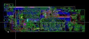
The PCB stack-up determines the relationship between signal layers, power planes, and ground planes. A properly designed stack-up can improve signal integrity, power integrity, electromagnetic compatibility, and manufacturing consistency.
When designing a multilayer PCB, engineers should consider:
- Number of signal layers
- Power and ground plane arrangement
- Dielectric thickness
- Copper thickness
- Material Dk and Df
- Controlled impedance requirements
- Thermal requirements
- Manufacturing tolerances
A stable and symmetrical stack-up can also help reduce PCB warpage and improve mechanical reliability during lamination and subsequent manufacturing processes.
Material Selection for High-Frequency and High-Speed PCBs
The selection of PCB Materials becomes particularly important when designing high-frequency and high-speed electronic products.
Conventional FR-4 materials are suitable for many applications, but specialized low-loss materials may be required for demanding high-frequency circuits.
The material selection should consider the operating frequency, signal speed, dielectric constant, dissipation factor, thermal requirements, manufacturing process, and overall product cost.
For multilayer hybrid boards, different materials may sometimes be combined to achieve a balance between electrical performance and manufacturing cost.
However, combining materials with different thermal expansion characteristics and resin systems introduces additional manufacturing challenges.
Therefore, material compatibility and lamination behavior must be carefully evaluated before production.
Manufacturing Considerations for Multilayer High-Frequency PCBs
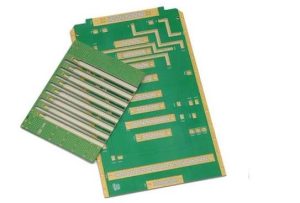
Kingda’s experience with high-precision PCB manufacturing shows that multilayer high-frequency boards require careful control of several manufacturing parameters.
During lamination, resin flow must be properly controlled to achieve stable dielectric thickness and reliable bonding between layers.
The following factors are particularly important:
- Prepreg selection
- Resin content
- Lamination temperature
- Lamination pressure
- Heating and cooling rates
- Material compatibility
- Board thickness
- Registration accuracy
- Copper distribution
- Resin flow characteristics
When different laminate materials are combined, controlling the bonding interface becomes more challenging.
Therefore, material selection, stack-up design, lamination parameters, and board structure should be evaluated as an integrated system.
Proper control of these factors can help reduce delamination, warpage, dimensional instability, and other reliability problems.
Conclusion
The continued development of electronic products is driving PCB technology toward higher density, higher frequency, faster signal transmission, and more sophisticated multilayer structures.
Traditional PCB manufacturing technologies remain important, but advanced applications such as HDI PCB, High-Frequency PCB, and High-Speed PCB require more precise materials, equipment, and process control.
In particular, Copper-Clad Laminate (CCL) selection, multilayer stack-up design, controlled-impedance routing, drilling accuracy, lamination, and etching all have a direct influence on the performance and reliability of the finished PCB.
For high-speed communication and electronic applications, Impedance Control must be considered from the design stage and maintained throughout the manufacturing process.
Kingda focuses on providing reliable PCB manufacturing solutions for high-density, high-frequency, and high-speed applications. Through careful material selection, precise manufacturing processes, controlled impedance management, and comprehensive quality control, Kingda aims to provide high-performance PCB solutions that meet the increasingly demanding requirements of modern electronic products.