What Is a 4 Layer PCB?
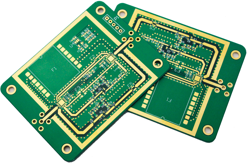
A 4 Layer PCB is a multilayer printed circuit board consisting of four conductive copper layers separated by insulating dielectric materials. Compared with a standard two-layer PCB, a four-layer design provides additional routing space, dedicated power and ground planes, improved signal integrity, and greater design flexibility.
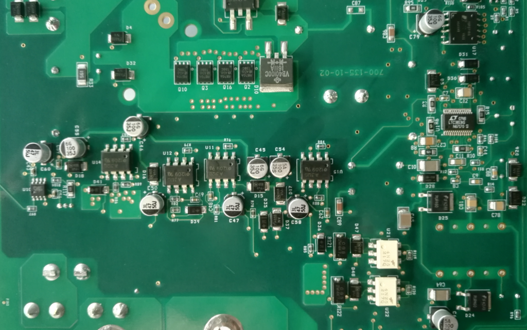
A typical four-layer PCB is constructed by laminating copper layers, dielectric materials, and prepreg under controlled temperature and pressure. The resulting structure forms a mechanically stable circuit board capable of supporting increasingly complex electronic designs.
Four-layer boards are widely used because they provide an effective balance between electrical performance, design complexity, manufacturing cost, and mechanical reliability. They are suitable for applications requiring higher routing density, controlled impedance, power distribution, electromagnetic interference management, or mixed-signal performance.
For customers developing products from prototype to production, a professional PCB Manufacturing partner can also help optimize layer stackups, material selection, copper weight, drilling, and manufacturability before production begins.
Common 4 Layer PCB Stackups
The stackup defines the order of signal, power, and ground layers inside a PCB. Choosing the correct stackup is critical for signal integrity, impedance control, power distribution, and electromagnetic compatibility.
Signal – Ground – Power – Signal
This is one of the most commonly used stackups for four-layer boards.
The two external layers are primarily used for signal routing, while the internal layers provide dedicated ground and power planes. This configuration simplifies power distribution and creates a stable reference plane for high-speed signals.
The close relationship between signal and ground layers can help reduce electromagnetic interference and improve controlled-impedance performance. It is suitable for general-purpose digital circuits, embedded systems, industrial electronics, and many mixed-signal applications.
For high-speed designs, the dielectric thickness between the signal and reference plane should be carefully controlled because it directly affects the required trace width for a specific impedance.
Signal – Ground – Ground – Signal
This configuration places ground planes between the two outer signal layers.
It is particularly useful when signal integrity and electromagnetic compatibility are important. The two external signal layers can reference adjacent ground planes, creating favorable conditions for controlled-impedance routing and reducing coupling between signal traces.
Although this structure does not provide a dedicated internal power plane, power can be distributed through copper pours or power traces on the signal layers.
This stackup can be suitable for Ethernet, GPS, communication, instrumentation, and other applications where stable high-speed signal transmission is important.
Signal – Ground – Signal – Ground
This stackup uses alternating signal and ground layers.
It is less common for general-purpose four-layer boards because it provides less convenient power distribution. However, it can be useful when sensitive analog or high-speed signals require strong electromagnetic shielding.
Placing signal layers adjacent to ground reference layers can help reduce unwanted coupling and provide a controlled return-current path. It may therefore be considered for noise-sensitive circuits or applications operating in electrically challenging environments.
Signal – Power – Power – Signal
This configuration can be considered when a design requires multiple voltage rails.
Two internal power layers can support different supply voltages, while the external layers are used primarily for signal routing. Ground can be implemented through copper pours or dedicated areas on the signal layers.
The appropriate configuration depends on the number of voltage domains, current requirements, signal-speed requirements, and overall PCB architecture.
How to Choose the Right 4 Layer PCB Stackup
There is no single stackup that is ideal for every four-layer PCB. The correct structure depends on the electrical and mechanical requirements of the product.
When selecting a stackup, PCB engineers should consider:
- Signal speed and frequency
- Controlled impedance requirements
- Power distribution
- Ground-plane continuity
- Electromagnetic compatibility
- Crosstalk requirements
- Copper thickness
- Dielectric thickness
- Component density
- Thermal requirements
- Manufacturing cost
For high-speed applications, maintaining a continuous reference plane beneath critical signal traces is especially important. The return current should have a low-impedance path, and unnecessary reference-plane discontinuities should be avoided.
The selection of core and prepreg materials also affects impedance, dielectric thickness, thermal performance, and manufacturing consistency.
Advantages of 4 Layer PCBs
A four-layer PCB offers several advantages over a conventional two-layer design.
Greater Routing Capacity
Four conductive layers provide substantially more routing space than a two-layer board. Designers can distribute signals across multiple layers while reserving internal planes for power and ground.
This makes it easier to accommodate dense component layouts and increasingly complex circuits without dramatically increasing board size.
Improved Signal Integrity
A dedicated ground plane provides a stable reference for high-speed signals and helps create predictable return-current paths.
With appropriate stackup design and impedance control, four-layer boards can provide better signal integrity than simpler two-layer structures.
Better Power Distribution
Internal power and ground planes can distribute power more efficiently across the board.
A well-designed power distribution structure can reduce voltage drops, minimize unwanted noise, and improve overall electrical performance.
Improved EMI and Crosstalk Control
Ground planes positioned close to signal layers can help contain electromagnetic fields and reduce unwanted coupling.
This is particularly beneficial for high-speed digital, communication, industrial control, and mixed-signal products.
Better Thermal Performance
Additional copper layers can contribute to heat spreading. Thermal vias can also transfer heat from surface components into internal copper areas.
The actual thermal benefit depends on copper thickness, copper area, component power dissipation, thermal vias, board construction, and enclosure design.
Stronger Mechanical Structure
The additional copper and dielectric layers contribute to the overall structural integrity of the PCB.
A properly laminated four-layer board provides a stable platform for component assembly and long-term operation.
4 Layer PCB Materials
Material selection has a direct influence on electrical performance, thermal reliability, mechanical strength, and manufacturing cost.
FR-4
Standard FR-4 is the most common material for general-purpose four-layer PCBs. Different FR-4 grades are available with different glass-transition temperatures, dielectric characteristics, and thermal properties.
For applications operating at elevated temperatures or requiring greater reliability, high-Tg FR-4 may be preferable.
High-Tg Materials
High-Tg materials are designed for applications requiring improved thermal stability.
They can be useful for industrial electronics, power electronics, automotive electronics, and products exposed to repeated thermal cycling.
High-Speed and High-Frequency Materials
For demanding high-speed or RF applications, specialized low-loss materials may be required.
Material selection should consider dielectric constant, dissipation factor, frequency range, thermal stability, and manufacturing requirements.
GOPCBA’s current PCB capability information includes standard and high-performance FR-4 materials as well as RF materials such as Rogers and Taconic options.
Halogen-Free Materials
Halogen-free PCB materials can be selected when environmental, regulatory, or product-specific requirements call for alternative flame-retardant systems.
The appropriate material should be selected according to the application’s electrical, thermal, mechanical, and compliance requirements.
4 Layer PCB Manufacturing Process
A reliable 4 Layer PCB Fabrication process requires accurate control of materials, imaging, lamination, drilling, plating, etching, surface finishing, and inspection.
1. Engineering Review
The manufacturing process begins with engineering verification of the customer’s Gerber files, drill files, stackup information, specifications, and other production data.
Design-for-manufacturing review can identify potential problems before fabrication and reduce the risk of production delays or repeated prototypes.
2. Inner Layer Imaging and Etching
The inner copper layers are processed according to the circuit pattern.
After imaging and etching, the copper pattern is inspected to verify trace width, spacing, registration, and other critical parameters.
3. Lamination
The inner layers are combined with prepreg and copper foil.
Controlled temperature, pressure, and time are used to create a stable multilayer structure. Proper lamination is essential for dimensional stability and reliable electrical performance.
4. Drilling
Through-holes are created using mechanical drilling.
Depending on the design, additional technologies such as laser drilling may be required for microvias or advanced HDI structures.
5. Copper Plating
The drilled holes are metallized to establish electrical connections between the appropriate copper layers.
Plating thickness and uniformity are important factors in determining long-term reliability.
6. Outer Layer Imaging and Etching
The external copper layers are patterned according to the PCB design.
Production controls are used to maintain accurate trace geometry and registration.
7. Solder Mask and Silkscreen
Solder mask protects exposed copper from oxidation and helps prevent solder bridging during assembly.
Silkscreen is used to identify component references, polarity markings, logos, and other production information.
8. Surface Finish
Depending on the application, common finishes include HASL, lead-free HASL, ENIG, OSP, immersion tin, immersion silver, and other specialized finishes.
The appropriate finish depends on solderability, environmental conditions, component requirements, shelf life, and cost.
9. Electrical Testing and Inspection
Finished boards can undergo automated optical inspection, electrical testing, dimensional inspection, and other quality-control procedures.
For complex or high-reliability applications, additional inspection and testing may be required.
Key Factors Affecting 4 Layer PCB Cost
The cost of a Custom PCB Manufacturing project depends on several technical and commercial factors.
Board Size and Quantity

Larger boards consume more material and may reduce panel utilization.
At the same time, larger production quantities generally improve manufacturing efficiency and reduce the average cost per PCB.
Material Selection
Standard FR-4 is usually more economical than high-performance materials.
High-Tg, low-loss, RF, halogen-free, and other specialized materials can increase material and processing costs.
Copper Weight
Higher copper weight requires additional copper and may require different plating and etching processes.
The required copper thickness should therefore be selected according to current capacity, thermal requirements, and design constraints rather than simply maximizing copper thickness.
Controlled Impedance
Controlled-impedance PCBs require accurate control of trace geometry and dielectric thickness.
Engineering verification and additional testing may increase manufacturing costs, but these processes are important for high-speed and RF applications.
Drilling Requirements
Standard through-holes are generally more economical than advanced drilling structures.
Blind vias, buried vias, microvias, and HDI structures add manufacturing steps and increase fabrication complexity.
Surface Finish
Different surface finishes have different material and processing costs.
ENIG, for example, may cost more than conventional HASL but can provide advantages for fine-pitch components and specific reliability requirements.
4 Layer PCB vs. 2 Layer PCB
The main difference between two-layer and four-layer PCBs is the amount of routing and reference-plane space available.
A two-layer PCB can be an excellent choice for relatively simple circuits with moderate routing density and limited high-speed requirements.
A four-layer PCB becomes more attractive when the design requires:
- Higher routing density
- Dedicated ground or power planes
- Controlled impedance
- Better signal integrity
- Improved EMI performance
- More compact layouts
- More complex mixed-signal circuits
- Better power distribution
Although four-layer PCBs generally cost more than two-layer boards, the additional manufacturing cost can be justified when the electrical and mechanical advantages reduce design complexity and improve product performance.
When Should You Use a 4 Layer PCB?
A four-layer PCB is often a practical choice when a two-layer board can no longer provide sufficient routing space or electrical performance.
Typical applications include:
- Industrial control equipment
- Embedded computing systems
- Communication devices
- Networking equipment
- Consumer electronics
- Automotive electronics
- Medical electronics
- IoT devices
- Power management systems
- Measurement and instrumentation equipment
The final decision should be based on the circuit complexity, operating frequency, power requirements, mechanical constraints, and production targets.
For projects requiring both fabrication and assembly, integrating PCB fabrication with PCB Assembly can also simplify supplier management and reduce coordination between separate manufacturing partners.
Why Choose GOPCBA for 4 Layer PCB Manufacturing?
GOPCBA provides integrated PCB manufacturing and electronic manufacturing services, supporting projects from PCB fabrication through assembly, testing, and final integration. The company’s current website describes capabilities covering PCB design, PCB manufacturing, component sourcing, SMT/THT assembly, testing, and box-build services.
One-Stop Manufacturing Support
GOPCBA can support customers throughout the product development and manufacturing cycle, from engineering review and PCB fabrication to component procurement, assembly, inspection, and testing.
This integrated approach can reduce communication gaps and simplify project management.
Flexible Production Capability
The company’s published PCB capability information covers multilayer boards, advanced materials, controlled impedance, different copper weights, multiple surface finishes, and advanced drilling options.
Engineering and Quality Control
Engineering review, DFM analysis, material verification, production inspection, and electrical testing help identify potential manufacturing issues before final delivery.
For PCB assembly projects, GOPCBA also describes a quality-control flow incorporating incoming inspection, SMT/THT assembly, AOI, X-ray, ICT/FCT, and outgoing quality control.
Prototype to Production
Whether you require a small prototype quantity, low-volume production, or larger manufacturing runs, a scalable manufacturing process can help reduce the transition from product development to production.
GOPCBA provides prototype PCB assembly as well as low-volume and high-volume manufacturing services.
Get a Quote for Your 4 Layer PCB Project
A reliable four-layer PCB manufacturer should be able to evaluate your complete design requirements rather than simply provide a board price.
To obtain an accurate quotation, customers should normally provide:
- Gerber files
- PCB specifications
- Board dimensions
- Layer count
- Material requirements
- Copper weight
- Board thickness
- Surface finish
- Quantity
- Special impedance requirements
- Via and drilling requirements
- Testing requirements
GOPCBA provides PCB manufacturing and assembly support for customers seeking a complete electronics manufacturing solution. For project-specific requirements, customers can contact the engineering and sales team directly through the GOPCBA contact page: https://www.gopcba.com/contact-us/.
Frequently Asked Questions
What are the advantages of a 4 layer PCB?
A four-layer PCB provides more routing space, improved signal integrity, better power distribution, stronger EMI control, and greater design flexibility than a conventional two-layer PCB.
What materials are used for 4 layer PCBs?
FR-4 is the most common material. Depending on the application, high-Tg, high-speed, RF, halogen-free, and other specialized materials can also be used.
What are the common 4 layer PCB stackups?
Common structures include Signal–Ground–Power–Signal, Signal–Ground–Ground–Signal, Signal–Ground–Signal–Ground, and Signal–Power–Power–Signal.
Is a 4 layer PCB better than a 2 layer PCB?
Not necessarily for every application. A two-layer PCB may be more economical for simple circuits, while a four-layer PCB is generally more suitable for dense, high-speed, mixed-signal, or EMI-sensitive designs.
Does a 4 layer PCB support controlled impedance?
Yes. With an appropriate stackup, controlled dielectric thickness, trace geometry, copper thickness, and manufacturing process, four-layer PCBs can support controlled-impedance designs.
How much does a 4 layer PCB cost?
The final price depends on board size, quantity, material, copper weight, thickness, surface finish, drilling, impedance requirements, and other manufacturing specifications.
How long does 4 layer PCB manufacturing take?
Production time varies according to board complexity, material availability, quantity, testing requirements, and manufacturing technology. The actual lead time should be confirmed after reviewing the production files.
Can 4 layer PCBs be assembled after fabrication?
Yes. A four-layer PCB can be assembled using SMT, THT, or mixed-technology processes. Integrating fabrication and assembly through one supplier can simplify procurement and project management.
Can GOPCBA provide PCB assembly together with PCB fabrication?
Yes. GOPCBA presents itself as a one-stop PCB and PCBA manufacturing provider, covering PCB fabrication, component sourcing, SMT/THT assembly, testing, and related services.
Start Your 4 Layer PCB Project
A well-designed four-layer PCB provides an effective combination of routing capacity, electrical performance, mechanical stability, and manufacturing cost.
From material selection and stackup design to impedance control, drilling, surface finishing, inspection, and testing, every manufacturing detail can affect final PCB performance.
GOPCBA supports customers with integrated PCB manufacturing and assembly solutions, helping transform PCB designs into reliable manufactured products. Whether you are developing a prototype, preparing for low-volume production, or planning a larger manufacturing program, professional engineering support and controlled production processes can help improve quality, reduce manufacturing risks, and accelerate time to market.
Start your 4 layer PCB project with GOPCBA today.