After the PCB manufacturing process is completed, the next major stage is PCB Assembly (PCBA). PCB fabrication creates the board structure, conductive layers, pads, vias, and other interconnections, while PCB assembly installs electronic components and forms the electrical and mechanical connections required for a functional electronic product.
As electronic devices become smaller, more powerful, and more highly integrated, modern PCB Assembly requires precise process control, automated equipment, engineering expertise, and comprehensive inspection. From solder paste printing and SMT component placement to reflow soldering, AOI, X-ray inspection, and functional testing, every stage can influence the quality and reliability of the final product.
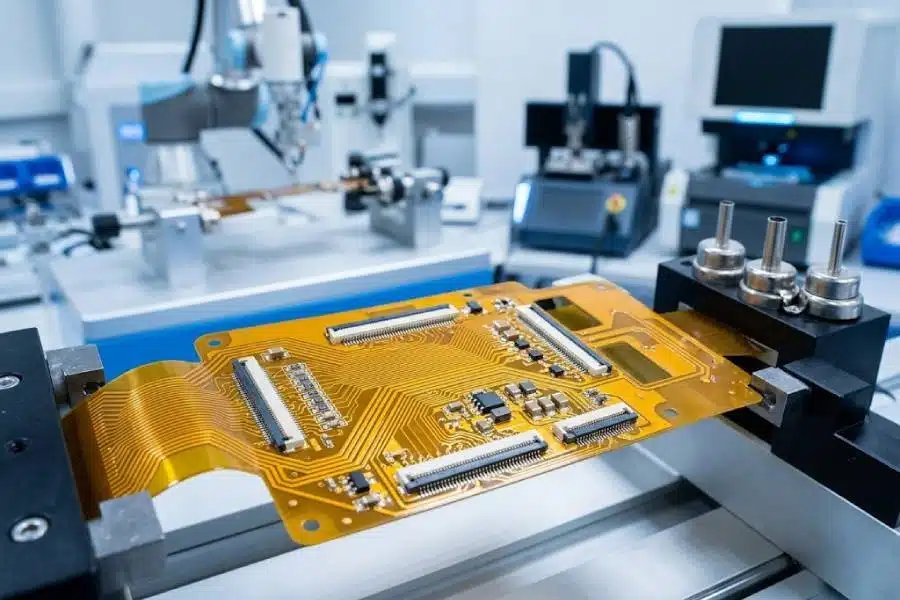
A typical PCB assembly workflow can be summarized as:
PCB Fabrication → Component Sourcing → Solder Paste Printing → SPI → SMT Component Placement → Reflow Soldering → THT/Selective Soldering → AOI/X-Ray → ICT/FCT → Final Inspection
This article provides a professional overview of the PCB Assembly Process, including stencil preparation, solder-paste printing, SMT placement, reflow soldering, inspection, common defects, and the advantages of working with Kingda.
What Is the PCB Assembly Process?
PCB Assembly is the process of mounting electronic components onto a fabricated printed circuit board and creating reliable electrical and mechanical connections.
A complete PCBA manufacturing process may include:
- PCB and component preparation
- DFM/DFA engineering review
- Stencil preparation
- Solder-paste printing
- Solder-paste inspection
- SMT component placement
- Reflow soldering
- THT insertion and soldering
- AOI inspection
- X-ray inspection
- Electrical testing
- Functional testing
- Final inspection and packaging
The exact process depends on the PCB structure, component technology, production volume, and application requirements.
1. PCB Design Review and DFM/DFA
Before production starts, a professional PCB Assembly Manufacturer should review the customer’s design.
DFM (Design for Manufacturability) evaluates whether the PCB can be fabricated efficiently and reliably.
DFA (Design for Assembly) focuses on component placement and assembly feasibility.
Typical review points include:
- PCB thickness
- Pad dimensions
- Component spacing
- Solder-mask openings
- Fiducial marks
- Component footprints
- Thermal considerations
- Test points
- Panelization
- Assembly orientation
Early DFM/DFA analysis can identify manufacturing issues before they become expensive production problems.
Kingda provides DFM/DFA engineering support as part of its PCB and PCBA services, helping customers optimize PCB designs before fabrication and assembly. (gopcba.com)
2. Stencil Preparation
For SMT PCB Assembly, the stencil is an important tool used to transfer solder paste to PCB pads.
A PCB stencil is a thin metal sheet containing accurately machined apertures that correspond to the solder-pad pattern.
Why Stencil Design Matters
Stencil design directly determines solder-paste transfer.
Important factors include:
- Stencil thickness
- Aperture size
- Aperture shape
- Pad geometry
- Component pitch
- Solder-paste type
A poorly designed stencil can cause:
- Insufficient solder
- Excess solder
- Solder bridging
- Poor solder-paste release
- Component-related solder defects
For fine-pitch devices, stencil aperture optimization is especially important.
3. Solder Paste Printing
Solder Paste Printing is one of the most critical processes in SMT assembly.
The PCB is aligned with the stencil using the assembly machine’s vision system. A squeegee then moves across the stencil and forces solder paste through the apertures onto the PCB pads.
The basic workflow is:
PCB Alignment → Stencil Alignment → Paste Printing → Stencil Separation → SPI Inspection
Stencil Alignment
Modern printers use fiducial marks to compensate for board position and rotation.
Accurate registration is essential for:
- Fine-pitch ICs
- BGA
- QFN
- 0201/01005 components
- High-density PCB assemblies
Squeegee Pressure
Squeegee pressure must be sufficient to transfer solder paste through stencil apertures while avoiding excessive spreading.
Too much pressure can lead to:
- Paste smearing
- Paste leakage
- Stencil wear
- Printing inconsistency
Too little pressure can leave solder paste inside the stencil apertures.
The correct value depends on the stencil, solder paste, board, and printing equipment.
Squeegee Speed
Squeegee speed affects the quality of solder-paste transfer.
If the speed is too high, small apertures may not fill properly. If it is too low, production efficiency can decrease.
The optimal speed should be determined through process qualification.
4. Stencil Separation and Cleaning
After printing, the stencil must separate from the PCB without pulling solder paste away from the pads.
Controlled stencil separation helps maintain consistent solder deposits.
Regular stencil cleaning is also essential because accumulated solder paste can block apertures and reduce printing accuracy.
Common cleaning methods include:
- Dry cleaning
- Wet cleaning
- Vacuum cleaning
- Solvent-assisted cleaning
The stencil should also be periodically inspected for:
- Blocked apertures
- Damaged apertures
- Contamination
- Warping
- Surface damage
5. Solder Paste Composition and Storage
Solder paste generally consists of metal solder powder suspended in a flux system.
Common lead-free alloys include SAC305 and other SAC-family alloys.
Solder Powder
The solder-powder size is selected according to:
- Component pitch
- Stencil aperture dimensions
- Printing requirements
- Assembly process
Smaller packages may require finer solder-powder grades.
Flux
Flux helps:
- Remove surface oxides
- Promote solder wetting
- Support reliable solder-joint formation
Solder Paste Rheology
Solder paste has complex non-Newtonian flow behavior.
It needs to:
- Flow through stencil apertures during printing
- Maintain shape after deposition
- Remain stable before component placement
Solder Paste Storage
Proper storage is essential to maintain solder-paste performance.
Manufacturers should control:
- Storage temperature
- Storage time
- Container sealing
- Moisture exposure
- Paste warming and conditioning
The exact requirements should follow the solder-paste manufacturer’s datasheet rather than using one universal storage temperature.
6. SMT Component Placement
After solder paste is printed, components are installed using automated pick-and-place machines.
Modern placement equipment uses vision systems to identify component position and orientation.
Typical components include:
- Resistors
- Capacitors
- Diodes
- ICs
- BGA
- QFN
- CSP
- LGA
- Connectors
- Sensors
- Power devices
Placement Accuracy
Placement accuracy becomes increasingly important as component size decreases.
High-density designs may contain:
- 01005 components
- Fine-pitch ICs
- Micro-BGA
- QFN
- CSP
The placement system must accurately compensate for PCB and component tolerances.
Fiducial Recognition
Fiducial marks provide fixed visual references.
The placement machine uses these points to determine:
- PCB position
- Board rotation
- Panel alignment
- Local registration
This ensures accurate component placement.
7. Reflow Soldering
After component placement, the PCB enters the reflow soldering process.
The board moves through a temperature-controlled reflow oven where the solder paste melts and forms permanent solder joints.
The reflow profile usually consists of:
Preheat → Soak → Reflow → Cooling
Preheat
The temperature increases gradually to reduce thermal stress and prepare the assembly for reflow.
Soak
The assembly reaches a more uniform temperature before the solder reaches the liquidus phase.
Reflow
The temperature rises above the solder alloy’s melting point, allowing solder to wet the pads and component terminals.
For common lead-free SAC solder alloys, peak temperatures are often around 230–250°C, but the correct profile depends on the solder paste, PCB construction, and component requirements.
Cooling
Controlled cooling allows the solder to solidify and helps form stable solder joints.
8. Common Reflow Soldering Defects
Solder Bridging
A solder bridge occurs when solder unintentionally connects neighboring pads.
Common causes include:
- Excessive solder paste
- Poor stencil design
- Component misalignment
- Insufficient pad spacing
- Incorrect reflow conditions
Solutions include:
- Optimizing stencil apertures
- Improving paste printing
- Increasing placement accuracy
- Optimizing reflow parameters
Tombstoning
Tombstoning occurs when one side of a small passive component lifts off the PCB during reflow.
It can result from:
- Uneven heating
- Unequal solder-paste volume
- Pad asymmetry
- Placement variation
Cold Solder Joints
A poor solder joint can result from insufficient wetting or an unsuitable thermal profile.
Potential causes include:
- Insufficient heat
- Surface contamination
- Incorrect reflow settings
- Material incompatibility
Solder Voiding
Voids can form inside solder joints during reflow.
Excessive voiding can be important for power and thermal connections.
Stencil design, solder paste, pad geometry, and reflow parameters should be optimized according to the application.
9. THT and Selective Soldering
Although SMT dominates modern electronics manufacturing, Through-Hole Technology (THT) remains important for mechanically demanding components.
Typical THT components include:
- Connectors
- Transformers
- Relays
- Large capacitors
- Power components
For mixed assemblies, manufacturers may use:
- Selective soldering
- Wave soldering
- Manual soldering
Selective soldering allows specific through-hole components to be soldered while minimizing thermal exposure to nearby SMT components.
10. Solder Paste Inspection
SPI (Solder Paste Inspection) verifies solder-paste quality before component placement.
SPI systems can measure:
- Paste volume
- Paste height
- Paste area
- Paste position
- Printing consistency
Early detection of printing problems can prevent larger assembly defects downstream.
Kingda lists 3D SPI among its PCB assembly inspection capabilities. (gopcba.com)
11. Automated Optical Inspection
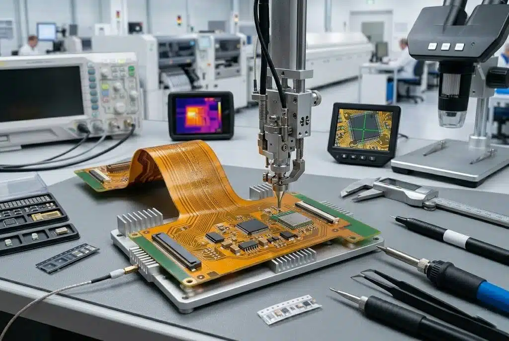
AOI (Automated Optical Inspection) uses high-resolution cameras and software to inspect assembled PCBs.
AOI can detect:
- Missing components
- Incorrect components
- Component misalignment
- Polarity errors
- Solder bridges
- Tombstoning
- Visible solder defects
AOI provides fast and repeatable inspection and is particularly useful in high-volume PCBA production.
12. X-Ray PCB Inspection
Some solder joints cannot be inspected from the surface.
This applies especially to:
- BGA
- QFN
- LGA
- Bottom-terminated components
X-ray inspection can reveal:
- Voids
- Hidden bridges
- Insufficient solder
- Open joints
- Internal defects
- Component alignment problems
For high-reliability PCBA, X-ray can provide an additional inspection layer beyond AOI.
13. Electrical and Functional Testing
Visual inspection alone cannot verify whether the entire circuit functions correctly.
ICT
In-Circuit Testing (ICT) can check:
- Continuity
- Shorts
- Opens
- Component values
- Selected electrical parameters
Flying Probe Testing
Flying-probe testing is often suitable for:
- Prototypes
- Low-volume production
- Engineering validation
It can reduce the need for dedicated test fixtures.
Functional Testing
Functional Testing (FCT) powers the PCB and verifies actual system behavior.
Depending on the application, FCT can verify:
- Voltage
- Current
- Communication interfaces
- Sensors
- Displays
- Motors
- Power-management systems
- Wireless functions
PCB Assembly Quality Control
A professional PCB Assembly Manufacturer should apply quality control throughout the complete production process.
A typical quality flow is:
IQC → SPI → SMT/THT → AOI → X-Ray → ICT/FCT → OQC
Each stage checks a different aspect of product quality.
IQC
Incoming materials are inspected before production.
SPI
Solder-paste printing is verified before placement.
Process Inspection
SMT, THT, reflow, and selective-soldering processes are monitored.
AOI
Visible assembly defects are detected automatically.
X-Ray
Hidden solder joints are inspected.
ICT/FCT
Electrical and functional performance is verified.
OQC
The completed product receives final inspection before shipment.
How to Improve PCB Assembly Yield
Improving PCB assembly yield requires controlling the entire manufacturing process rather than focusing on only one piece of equipment.
Optimize PCB Design
A production-friendly layout reduces manufacturing complexity.
Perform DFM/DFA Early
Identify potential problems before fabrication.
Control Solder-Paste Printing
Printing defects can propagate into multiple downstream soldering problems.
Optimize Reflow Profiles
Thermal profiles should be validated for each PCB and solder-paste combination.
Use SPI and AOI
Early inspection enables rapid correction of process drift.
Use X-Ray for Hidden Joints
This is particularly important for BGA and other bottom-terminated components.
Establish Process Traceability
Production data should be recorded so defects can be traced back to their source.
Kingda PCB Assembly Advantages
For companies seeking a professional PCB Assembly Manufacturer, Kingda provides an integrated manufacturing solution covering PCB fabrication, component sourcing, SMT, THT/DIP, inspection, testing, and finished-product assembly. (gopcba.com)
One-Stop PCB and PCBA Manufacturing
Kingda integrates:
PCB Design → PCB Fabrication → Component Procurement → SMT/THT → Inspection → Testing → Finished Product Assembly
This reduces the need for customers to coordinate multiple suppliers. (gopcba.com)
Advanced SMT Assembly
Kingda’s published capabilities support advanced component packages including:
- 01005
- BGA
- QFN
- CSP
- LGA
- Fine-pitch ICs
- PoP
The company reports support for 0.35 mm-pitch BGA and fine-pitch components down to 0.38 mm pitch. (gopcba.com)
SMT, THT, and Mixed Technology
Kingda provides:
- SMT assembly
- THT/DIP assembly
- Mixed-technology assembly
- Wave soldering
- Selective soldering
- Manual soldering
This allows customers to build complex PCBAs containing both miniature SMD components and mechanically robust through-hole parts. (gopcba.com)
Comprehensive Inspection
Kingda’s published inspection and testing capabilities include:
- 3D SPI
- AOI
- X-Ray
- First Article Inspection
- ICT
- FCT
- Customized testing
Its published PCBA quality flow includes incoming inspection, SPI, SMT/THT assembly, AOI, X-ray, electrical testing, functional testing, and final quality inspection. (gopcba.com)
DFM/DFA Engineering Support
Kingda provides engineering support covering:
- DFM
- DFA
- PCB design review
- BOM review
- Component selection
- Panelization
- Manufacturing optimization
These services help identify assembly problems before production begins. (gopcba.com)
Component Sourcing
Kingda provides component procurement and BOM management, helping customers coordinate component availability, sourcing, and production scheduling. (gopcba.com)
Quality Certifications
Kingda reports:
- IATF 16949:2016
- ISO 13485:2016
- ISO 9001:2015
- ISO 14001:2015
- UL
The company also states that it is an IPC member. (gopcba.com)
These quality systems support applications in automotive, medical, industrial, communication, power, and other demanding electronics sectors.
Prototype to Mass Production
Kingda supports:
Prototype → Low Volume → Pilot Production → High Volume Production
This allows customers to develop, validate, and scale PCB assembly projects through one manufacturing partner. (gopcba.com)
How to Choose a PCB Assembly Manufacturer
When selecting a PCB Assembly Supplier, consider the following:
Manufacturing Capabilities
Check whether the supplier supports:
- SMT
- THT
- Mixed technology
- BGA
- Fine pitch
- Flexible PCB
- Rigid-flex PCB
- HDI PCB
- High-speed PCB
Engineering Support
Look for:
- DFM
- DFA
- BOM review
- PCB design review
- Test-point optimization
- Manufacturing engineering
Quality Control
Confirm the availability of:
- SPI
- AOI
- X-ray
- ICT
- FCT
Component Procurement
Evaluate:
- Supply-chain resources
- Component verification
- Alternative components
- Inventory management
- Lead-time control
Traceability
The supplier should be able to track:
Component → PCB → Assembly Process → Inspection → Testing → Shipment
Conclusion
The PCB Assembly Process is a highly coordinated manufacturing workflow that combines engineering, material management, precision component placement, soldering, inspection, and testing.
The key stages can be summarized as:
DFM/DFA → Stencil Preparation → Solder Paste Printing → SPI → SMT Placement → Reflow Soldering → THT/Selective Soldering → AOI/X-Ray → ICT/FCT → Final Inspection
Among these steps, solder paste printing, component placement, and reflow soldering have a particularly strong influence on solder-joint quality and production yield. At the same time, SPI, AOI, X-ray, ICT, and FCT provide multiple layers of quality verification.
For customers looking for an experienced PCB Assembly Manufacturer, Kingda provides integrated PCB fabrication, component procurement, SMT/THT assembly, DFM/DFA engineering, SPI, AOI, X-ray, ICT/FCT, prototype production, and volume manufacturing. (gopcba.com)
With quality certifications including IATF 16949, ISO 13485, ISO 9001, ISO 14001, and UL, Kingda can support demanding projects in automotive, medical, industrial, communication, AI, power, and consumer electronics. (gopcba.com)