In today’s fast-moving electronics industry, development schedules are becoming increasingly demanding. Engineers and product teams often need functional circuit boards within days rather than weeks to validate a design, solve urgent production problems, or meet a critical product launch deadline.
This is where Quick Turn PCB manufacturing becomes especially valuable.

A Quick Turn PCB is a printed circuit board manufactured and delivered through an accelerated production schedule. Compared with standard PCB fabrication, quick-turn manufacturing uses streamlined engineering review, readily available materials, prioritized production scheduling, automated manufacturing, and efficient inspection processes to shorten the overall lead time.
Quick-turn PCB services are widely used for PCB prototyping, engineering validation, low-volume production, emergency replacement boards, and time-sensitive product development.
For companies that need both PCB fabrication and assembly, an integrated Quick Turn PCB Assembly service can further shorten the development cycle by combining PCB manufacturing, component sourcing, SMT/THT assembly, inspection, and functional testing.
Kingda provides rapid PCB prototyping and quick-turn PCBA services, including PCB fabrication, component procurement, SMT and through-hole assembly, AOI, X-ray, ICT, FCT, and functional testing. Kingda currently publishes prototype lead-time options ranging from normal 2–3 days to expedited services under specific conditions. (GoPCBA)
What Is a Quick Turn PCB?
A Quick Turn PCB is a printed circuit board produced on an accelerated manufacturing schedule to reduce the time between design submission and finished PCB delivery.
Traditional PCB fabrication may require several weeks depending on board complexity, material requirements, production volume, and testing requirements. A quick-turn service compresses this timeline by optimizing each stage of production.
The basic workflow is:
Design Review → DFM Check → Material Preparation → PCB Fabrication → Drilling → Plating → Etching → Solder Mask → Surface Finish → Electrical Testing → Inspection → Shipment
For assembled boards, the process continues with:
Component Sourcing → Solder Paste Printing → SMT Placement → Reflow Soldering → AOI/X-Ray → THT Assembly → ICT/FCT → Final Inspection → Shipment
Quick-turn manufacturing does not mean eliminating essential quality-control steps. The objective is to remove unnecessary waiting time while maintaining appropriate manufacturing and inspection controls.
How Quick Turn PCB Manufacturing Works
Step 1: Design File Review
The manufacturing process begins when the customer submits the PCB production files.
Common files include:
- Gerber files
- ODB++
- Drill files
- PCB stackup information
- BOM
- Pick-and-place files
- Assembly drawings
- Special manufacturing requirements
The manufacturer performs a DRC and DFM review to identify potential problems before production begins.
Typical issues include:
- Insufficient clearance
- Incorrect drill sizes
- Inadequate annular rings
- Incorrect footprints
- Trace-width violations
- Solder-mask problems
- Missing manufacturing information
Resolving these issues before fabrication can prevent unnecessary delays.
Kingda provides engineering design review and DFM support as part of its PCB manufacturing and assembly workflow. (GoPCBA)
Step 2: Material Selection and Preparation
Quick-turn PCB manufacturers typically keep common materials available to minimize procurement delays.
Common materials include:
FR-4, High-Tg FR-4, Aluminum PCB Materials, Polyimide, High-Frequency Laminates, and Other Specialty Materials
For standard prototype boards, FR-4 is often the fastest material choice because of its broad availability.
Specialty materials may require additional procurement time, especially when the design requires:
- High-frequency laminates
- Low-loss dielectric materials
- Heavy copper
- Metal-core substrates
- Flexible materials
- Advanced HDI structures
Step 3: Inner-Layer Imaging
For multilayer PCBs, the internal copper layers must be accurately transferred from the design data to the PCB material.
Modern PCB manufacturers may use Laser Direct Imaging (LDI) technology to improve accuracy and reduce conventional phototool-related delays.
Step 4: Lamination and Drilling
Multilayer boards are laminated under controlled heat and pressure.
After lamination, CNC drilling machines create:
- Through-holes
- Vias
- Component holes
- Mechanical holes
For high-density designs, laser drilling may also be used to create microvias.
The complexity of drilling has a direct effect on quick-turn lead time. A simple two-layer PCB is generally easier to accelerate than a complex HDI board with blind and buried vias.
Step 5: Copper Plating and Etching
After drilling, the holes are metallized to establish electrical connections between conductive layers.
The board then undergoes imaging and etching to create the required copper traces.
Process control is particularly important for:
- Fine-line PCBs
- High-speed PCBs
- Controlled-impedance boards
- HDI PCBs
Step 6: Solder Mask and Surface Finish
A solder mask protects exposed copper and helps prevent solder bridges during PCB assembly.
Common surface finishes include:
- HASL
- Lead-free HASL
- ENIG
- OSP
- Immersion Tin
- Immersion Silver
- ENEPIG
The appropriate finish depends on the board’s application, component package, shelf-life requirements, and assembly process.
Step 7: Electrical Testing and Inspection
Before shipment, PCBs should undergo appropriate inspection and electrical testing.
Typical methods include:
AOI, Flying Probe Testing, Electrical Continuity Testing, and Visual Inspection
For assembled PCBs, additional methods can include:
SPI, AOI, X-Ray, ICT, and FCT
Kingda’s published quality-control workflow includes IQC → SPI → SMT/THT → AOI → X-Ray → ICT/FCT → OQC, allowing inspection and testing to be integrated throughout manufacturing rather than relying solely on final inspection. (GoPCBA)
Typical Quick Turn PCB Lead Times
Actual lead time depends on board complexity, material availability, production capacity, quantity, and testing requirements.
A practical reference is:
| Service | Typical Lead Time | Typical Application |
|---|---|---|
| Same-day / expedited | Several hours to 1 day | Critical engineering needs |
| 24–48 hours | 1–2 business days | Simple prototype PCBs |
| 3–5 days | 3–5 business days | Multilayer prototypes |
| 5–7 days | 5–7 business days | More complex PCB designs |
| Extended quick turn | 7+ days | HDI, rigid-flex, specialty materials |
These are general industry ranges rather than universal guarantees. The actual delivery date should always be confirmed with the manufacturer.
Kingda currently lists prototype production as normally 2–3 days, with an expedited option as fast as 12 hours under specific conditions. It also lists low-volume production at 3–5 days and volume production at 5–7 days, depending on project requirements. (GoPCBA)
Benefits of Quick Turn PCB Services
Faster Time to Market
The biggest advantage of Quick Turn PCB Manufacturing is reduced development time.
Instead of waiting several weeks for each engineering revision, teams may be able to complete multiple prototype cycles in a significantly shorter period.
This is especially valuable when:
- Product launch dates are fixed
- Customer demonstrations are approaching
- Engineering teams need physical validation
- Hardware and software development are happening simultaneously
Rapid Prototype Validation
A functional prototype allows engineers to evaluate:
- Electrical performance
- Signal integrity
- Power integrity
- Thermal behavior
- Component compatibility
- Mechanical fit
- Firmware integration
A faster prototype cycle means problems can be discovered earlier.
Reduced Development Risk
Manufacturing defects or design problems discovered during prototyping are usually easier and less costly to correct than problems discovered after mass production begins.
Quick Turn PCB Prototyping therefore acts as a risk-reduction tool as well as a manufacturing service.
Emergency Production Support
Quick-turn manufacturing can also be used when:
- A production PCB fails
- Replacement boards are urgently required
- A component change requires a new PCB revision
- Existing inventory is insufficient
- A field-replacement board is needed
Flexible Design Iteration
Hardware products rarely reach their final design in one revision.
Quick-turn fabrication supports a development loop of:
Design → Build → Test → Analyze → Improve
This approach helps engineering teams make decisions using real hardware data instead of relying entirely on simulation.
Quick Turn PCB vs. Standard PCB Fabrication
| Factor | Quick Turn PCB | Standard PCB Fabrication |
|---|---|---|
| Lead Time | Hours to several business days | Several days to weeks |
| Main Purpose | Prototypes and urgent production | Planned production |
| Order Quantity | Small to medium | Medium to high |
| Unit Cost | Generally higher | Generally lower |
| Material Selection | Often focuses on stocked materials | Broader material options |
| Engineering Support | High priority | Standard workflow |
| Best For | Prototypes, urgent replacements | Planned production |
| Production Planning | Priority scheduling | Regular scheduling |
The fundamental trade-off is time versus cost.
Quick-turn boards may have a higher unit price because manufacturers prioritize the job and may incur additional scheduling, labor, material, and logistics costs.
For a large-volume project with a predictable schedule, conventional production is often more economical.
Applications of Quick Turn PCBs
Electronics Prototyping
This is one of the most common applications of Quick Turn PCB Services.
Startups, OEMs, engineering departments, and R&D teams can quickly convert CAD designs into physical boards.
Automotive Electronics
Quick-turn PCBs are useful for developing:
- ADAS modules
- ECUs
- Sensor systems
- Battery-management systems
- Infotainment systems
- Vehicle communication modules
Automotive engineers can use fast prototypes for hardware validation and HIL testing.
Aerospace and Defense
Aerospace projects often require extensive testing and strict development schedules.
Quick prototypes can support:
- Avionics
- Navigation systems
- Communication equipment
- Radar electronics
- Test instrumentation
Medical Devices
Prototype PCBs can help medical-device engineering teams validate electronics before formal regulatory and product qualification stages.
Applications include:
- Patient monitoring
- Diagnostic equipment
- Portable medical devices
- Laboratory equipment
Consumer Electronics
Smartphones, wearables, IoT products, smart-home equipment, and portable devices often require multiple design iterations.
Fast PCB fabrication can accelerate those development cycles.
Industrial Electronics
Quick-turn boards are also useful for:
- Industrial controllers
- PLC interfaces
- Test equipment
- Robotics
- Power electronics
- Sensor systems
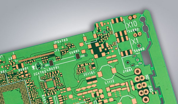
Design Considerations for Quick Turn PCBs
Good PCB design is one of the most effective ways to reduce manufacturing delays.
Use Standard Materials
For rapid production, standard materials such as FR-4 are generally easier to source than specialty laminates.
Use Standard Layer Counts
Two-layer and four-layer boards are usually easier to manufacture quickly than complex multilayer designs.
Every additional layer may introduce more:
- Lamination
- Imaging
- Drilling
- Registration
- Inspection
Avoid Unnecessary Tight Tolerances
Very narrow traces, microvias, unusual holes, and extreme dimensional tolerances can increase manufacturing complexity.
Use advanced specifications only when they are technically necessary.
Prepare Complete Gerber Files
Incomplete or incorrect files can eliminate the time savings of quick-turn manufacturing.
Before submission, verify:
- Layer count
- Board outline
- Drill files
- Copper layers
- Solder mask
- Silkscreen
- Stackup
- Special requirements
Confirm Stackup Requirements Early
For high-speed or controlled-impedance designs, the stackup must be established before manufacturing.
Important parameters include:
- Dielectric thickness
- Copper thickness
- Dk
- Trace width
- Trace spacing
- Target impedance
Changing these requirements after production begins can significantly affect lead time.
Cost Factors in Quick Turn PCB Manufacturing
Several factors influence the cost of Quick Turn PCB Manufacturing.
Lead Time
The shorter the requested lead time, the more likely priority scheduling or expedited logistics will increase cost.
Layer Count
A two-layer PCB is usually less expensive and faster to manufacture than an eight-layer PCB.
PCB Size
Larger boards consume more material and may reduce panel utilization.
Quantity
Very small quantities can have higher unit costs because engineering and setup costs are distributed across fewer boards.
Surface Finish
HASL is generally economical, while finishes such as ENIG or ENEPIG may cost more but provide advantages for fine-pitch components and specific applications.
Special Features
Additional costs may result from:
- Controlled impedance
- Blind/buried vias
- HDI
- Heavy copper
- Edge plating
- Countersinks
- Castellated holes
- Special materials
Shipping
For extremely urgent orders, expedited transportation can represent a meaningful portion of the total project cost.
How to Reduce Quick Turn PCB Cost and Lead Time
1. Choose Standard Materials
Use stocked materials wherever possible.
2. Simplify the Design
Avoid unnecessary layers, special finishes, and complex via structures.
3. Provide Complete Documentation
Complete design files allow engineering teams to start the review immediately.
4. Use Standard Surface Finishes
Select HASL, lead-free HASL, ENIG, OSP, or another standard finish based on the actual application requirements.
5. Use PCB Panelization
For small boards, panelization can increase production efficiency and improve machine utilization.
6. Combine PCB Fabrication and Assembly
Using one supplier for both PCB fabrication and Quick Turn PCB Assembly can reduce coordination and shipping delays.
Kingda provides PCB fabrication, component sourcing, SMT/THT assembly, testing, and turnkey PCBA through an integrated manufacturing model. (GoPCBA)
What to Look for in a Quick Turn PCB Manufacturer
A fast PCB supplier should provide more than a short advertised lead time.
Engineering Support
Look for:
DFM + DFA + BOM Review + Stackup Review + Manufacturing Feedback
Manufacturing Capability
The manufacturer should be able to support the PCB technology required by your project.
Component Procurement
For assembled boards, component availability is often one of the biggest factors affecting lead time.
Kingda maintains supplier relationships with major distributors including Digi-Key, Mouser, and Element14, according to its published PCB assembly information. (GoPCBA)
Inspection and Testing
Look for:
- SPI
- AOI
- X-Ray
- ICT
- FCT
- FAI
Quality Management
Kingda reports ISO 9001, ISO 13485, and IATF 16949 quality-management certifications and states that it maintains manufacturing traceability throughout the production lifecycle. (GoPCBA)
Kingda Quick Turn PCB Advantages
Rapid PCB Prototyping
Kingda provides rapid PCB prototyping for projects requiring short development cycles. Its published prototype service offers no MOQ, SMT/THT assembly, fine-pitch component insertion, and 4–7-day quick-turn prototyping. (GoPCBA)
Fast Prototype Lead Time
Kingda currently publishes:
Prototype: 2–3 days normally
Fastest expedited prototype: 12 hours under specified conditions
Actual lead time depends on PCB specifications, component availability, quantity, and testing requirements. (GoPCBA)
Advanced SMT Capability
Kingda’s published prototype capabilities include:
- 01005
- 0201
- BGA
- QFN
- Fine-pitch components
- SMT
- THT
- Mixed assembly
It lists a minimum BGA pitch of 0.25 mm and IC assembly precision of approximately ±0.03 mm under its stated prototype capabilities. (GoPCBA)
Comprehensive Inspection
Kingda integrates:
3D SPI + AOI + X-Ray + FAI + ICT + FCT
into its production and inspection system. (GoPCBA)
Integrated PCB and PCBA Services
Kingda’s one-stop manufacturing model covers:
PCB Design → PCB Manufacturing → Component Procurement → SMT → DIP/THT → Testing → Finished Product Assembly
This reduces the number of suppliers involved in a prototype project and simplifies communication. (GoPCBA)
Support from Prototype to Mass Production
Kingda supports the manufacturing path from rapid prototyping and low-volume production to high-volume production, enabling customers to continue working with the same manufacturing partner as demand increases. (GoPCBA)
When Should You Choose Quick Turn PCB Services?
Quick Turn PCB Services are particularly appropriate when:
You are actively developing a prototype.
Multiple hardware iterations can be completed without waiting several weeks between revisions.
You have a fixed product deadline.
A rapid manufacturing cycle can help recover development time lost during design revisions.
You need working hardware for demonstration.
Rapid PCB production can support customer demonstrations, investor presentations, technical evaluations, and trade shows.
You require emergency replacement boards.
Fast manufacturing can reduce downtime when existing PCBs are unavailable.
Your design is still evolving.
Quick-turn production allows you to validate the current design before committing to larger production quantities.
For predictable, high-volume demand, standard PCB manufacturing remains the more economical option.
Quick Turn PCB for Prototype-to-Production Development
One of the most important benefits of a strong Quick Turn PCB Manufacturer is the ability to support the complete product lifecycle.
A typical development path is:
Prototype → Engineering Validation → Design Revision → Pilot Production → Low Volume → High Volume Production
Using one manufacturing partner throughout this process can reduce:
- Supplier qualification time
- Design-transfer risk
- Process inconsistencies
- Component sourcing changes
- Communication overhead
Kingda’s published services cover rapid PCB prototyping, low-volume production, volume production, turnkey PCB assembly, component procurement, testing, and box-build assembly. (GoPCBA)
Conclusion
Quick Turn PCB manufacturing has become an essential solution for modern electronics development. By reducing fabrication and assembly lead times, engineers can validate designs faster, identify problems earlier, and accelerate the transition from concept to production.
A successful quick-turn program is not simply about making a PCB faster. It depends on the combination of:
Fast Engineering Review + DFM + Available Materials + Efficient PCB Fabrication + Reliable Component Sourcing + Automated Assembly + AOI/X-Ray + Electrical Testing
Kingda provides an integrated Quick Turn PCB and Quick Turn PCB Assembly solution covering PCB fabrication, component procurement, SMT/THT assembly, inspection, testing, and rapid prototyping. Its current published capabilities include no MOQ for prototypes, rapid prototype lead times, 01005/0201 component assembly, BGA support, AOI/X-ray inspection, ICT/FCT, and prototype-to-volume manufacturing. (GoPCBA)
For engineering teams, startups, OEMs, and electronics manufacturers working under tight deadlines, choosing a manufacturing partner with both speed and manufacturing depth can make a significant difference in development efficiency and time-to-market.