PCB prototype assembly is a critical stage in electronics product development. It transforms a PCB design into a physical, functional assembly that engineers can test, validate, modify, and prepare for production.
Whether you are developing a consumer electronic device, industrial controller, medical product, automotive system, IoT device, or aerospace application, a well-built prototype can reveal design and manufacturing problems before they become expensive production issues.
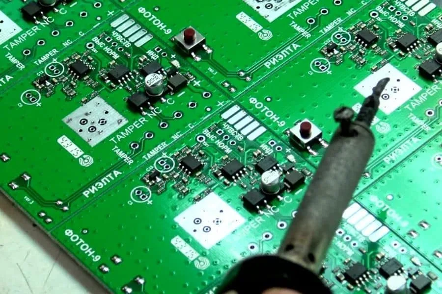
Unlike mass production, prototype PCB assembly emphasizes flexibility, rapid turnaround, engineering support, low-volume manufacturing, and fast design iteration. The goal is not simply to produce a small number of boards, but to create reliable physical prototypes that accurately represent the intended production design.
Kingda provides PCB prototype assembly, PCB fabrication, component procurement, SMT and through-hole assembly, inspection, programming, and functional testing. Its published prototype capabilities include no MOQ, 4–7-day quick-turn rapid prototyping, 01005 and 0201 components, BGA down to 0.25 mm pitch, AOI and X-ray inspection, ICT, FCT, and FAI. (GoPCBA)
What Is PCB Prototype Assembly?
A PCB prototype is an initial physical version of a PCB design created for testing and engineering validation before the product moves into larger-scale production.
PCB prototype assembly is the process of mounting electronic components onto that fabricated PCB according to the BOM, assembly drawings, and placement data.
The overall process connects:
Electronic Design → PCB Fabrication → Component Sourcing → PCB Assembly → Testing → Design Validation
PCB fabrication creates the physical circuit board, while PCB Assembly populates the board with components such as:
- Resistors
- Capacitors
- Diodes
- ICs
- Microcontrollers
- Connectors
- Sensors
- Power devices
- BGA and QFN packages
The completed prototype can then be evaluated for electrical, mechanical, thermal, firmware, and manufacturing performance.
Why Use Prototype PCB Assembly?
1. Verify Design Functionality
The primary purpose of Prototype PCB Assembly is to verify whether the physical circuit performs as intended.
Engineers can evaluate:
- Circuit functionality
- Power delivery
- Signal integrity
- Component compatibility
- Thermal behavior
- Communication interfaces
- Mechanical fit
- Firmware integration
A prototype provides much more practical information than simulation alone.
2. Accelerate Product Development
Fast prototyping allows engineering teams to shorten the time between design iterations.
A typical development cycle becomes:
Design → Prototype → Test → Improve → Prototype Again
The faster this cycle can be completed, the faster the final product can approach production readiness.
3. Identify Design Problems Early
Prototype manufacturing can expose issues such as:
- Incorrect footprints
- Component interference
- Insufficient spacing
- Thermal hotspots
- Power-integrity problems
- Signal crosstalk
- Connector misalignment
- Soldering problems
Correcting these problems during prototype development is generally much less costly than correcting them after mass production.
4. Support Firmware Development
For embedded electronic products, the physical prototype provides the hardware platform needed for:
- Firmware development
- Driver testing
- Communication testing
- Sensor calibration
- Programming
- Debugging
- Hardware-software integration
5. Prepare for Mass Production
Prototype assembly can also act as a manufacturing rehearsal.
By using processes similar to those planned for volume production, engineers can evaluate:
- Component placement
- Soldering
- Assembly yield
- Test procedures
- Panelization
- Manufacturing tolerances
- Component availability
This creates a smoother transition from Prototype PCB Assembly to mass production.
Types of PCB Prototype Assembly
Different PCB designs require different assembly methods.
Manual Prototype Assembly
Manual soldering can be suitable for:
- Very small quantities
- Simple boards
- Engineering modifications
- Early-stage experiments
- Components that are difficult to automate
It offers flexibility but is not ideal for dense or complex PCBs.
SMT Prototype Assembly
Surface Mount Technology (SMT) is widely used for modern prototype boards.
Advantages include:
- High component density
- Compact board designs
- Automated component placement
- Good repeatability
- Compatibility with fine-pitch devices
Through-Hole Prototype Assembly
Through-Hole Technology (THT) remains valuable for components requiring additional mechanical strength.
Typical examples include:
- Large connectors
- Transformers
- Power components
- Mechanical switches
Mixed Technology Assembly
Many prototypes combine SMT and THT components.
Mixed Technology PCB Assembly provides flexibility for designs that contain both fine-pitch SMDs and mechanically demanding through-hole components.
Kingda supports SMT, through-hole, and mixed assembly for prototype manufacturing. (GoPCBA)
PCB Prototype Assembly Process
Step 1: Design Review
The process starts with engineering review of the design data.
Typical files include:
- Gerber files
- BOM
- Pick-and-place file
- Assembly drawings
- Schematic
- PCB stackup
- Manufacturing requirements
Kingda’s engineering team reviews prototype designs before production to identify potential manufacturing problems and improve the efficiency of the prototype process. (GoPCBA)
Step 2: DFM and DFA Analysis
DFM (Design for Manufacturability) evaluates whether the PCB can be fabricated reliably.
DFA (Design for Assembly) evaluates whether components can be assembled efficiently.
Typical checks include:
- Trace width and spacing
- Pad dimensions
- Via sizes
- Component clearances
- Footprint accuracy
- Polarity
- Component orientation
- Solder-mask openings
Kingda provides DFMA support, combining Design for Manufacturing and Design for Assembly engineering analysis. (GoPCBA)
Step 3: PCB Fabrication
The bare PCB is manufactured according to the approved design.
Prototype boards may use:
- FR-4
- High-Tg FR-4
- HDI
- Flexible PCB
- Rigid-flex PCB
- High-frequency materials
- Metal-core PCB
For a prototype intended to transition into volume production, the fabrication process should be selected with the final production requirements in mind.
Step 4: Component Procurement
After the BOM is confirmed, components are sourced.
A professional PCB Component Sourcing process should evaluate:
- Manufacturer part numbers
- Availability
- Lifecycle status
- Package type
- Quantity
- Approved substitutes
- Supplier reliability
Kingda provides component procurement as part of its one-stop PCBA service and maintains an integrated sourcing and inventory-management system. (GoPCBA)
Step 5: Solder Paste Printing
For SMT assembly, solder paste is deposited onto PCB pads through a stencil.
The process controls:
- Stencil alignment
- Aperture dimensions
- Paste volume
- Printing pressure
- Printing speed
Poor solder-paste deposition can result in bridging, insufficient solder, and other defects.
Step 6: SMT Component Placement
Automated pick-and-place machines position components according to the placement file.
Kingda’s published prototype capabilities include:
01005 + 0201 + BGA + QFN + Fine-Pitch Components
The company lists a minimum BGA pitch of 0.25 mm and IC placement precision of approximately ±0.03 mm under its published prototype specifications. (GoPCBA)
Step 7: Reflow Soldering
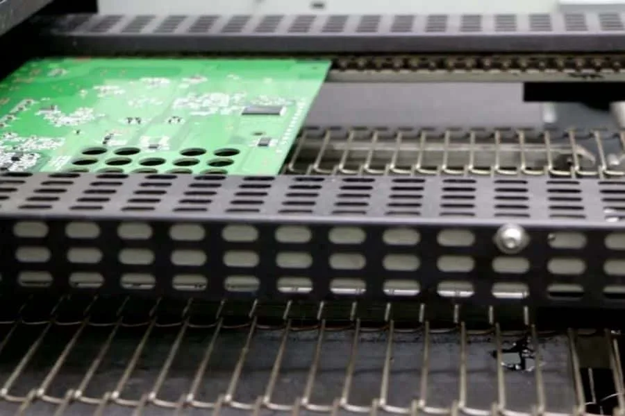
The assembled PCB passes through a controlled reflow oven.
The reflow profile must be optimized for:
- PCB material
- Solder paste
- Component types
- Board thickness
- Copper distribution
- Thermal sensitivity
Proper thermal control reduces defects such as tombstoning, cold solder joints, bridging, and component damage.
Step 8: Through-Hole Soldering
For THT components, manufacturers may use:
- Manual soldering
- Wave soldering
- Selective soldering
Kingda supports manual and automated through-hole insertion as well as wave and selective soldering. (GoPCBA)
Step 9: Inspection
Prototype boards should receive professional inspection even when the quantity is small.
AOI
Automated Optical Inspection (AOI) can detect:
- Missing components
- Incorrect components
- Component misalignment
- Polarity errors
- Solder defects
X-Ray
X-Ray Inspection is particularly useful for hidden solder joints such as BGA connections.
Kingda’s published prototype service includes 100% AOI and X-ray testing. (GoPCBA)
Step 10: Electrical and Functional Testing
After assembly, electrical testing verifies whether the circuit is connected correctly.
Depending on the application, testing may include:
- ICT
- Flying probe
- Functional testing
- Firmware programming
- Communication testing
- Power testing
- Sensor testing
Kingda provides ICT, FCT, IC programming, and customized testing for PCB assemblies. (GoPCBA)
Factors Affecting PCB Prototype Assembly Cost
The cost of Prototype PCB Assembly depends on several factors.
PCB Complexity
More layers, HDI structures, fine traces, and advanced materials generally increase manufacturing complexity.
Component Count
A board containing 20 components is considerably simpler to assemble than one containing several hundred components.
Component Package
Fine-pitch components, BGA, QFN, 01005, and other miniature packages require greater manufacturing precision.
Double-Sided Assembly
Assembling components on both PCB sides increases process complexity.
Testing Requirements
Basic AOI costs less than comprehensive testing involving:
- X-ray
- ICT
- FCT
- Environmental testing
- Programming
Component Availability
Specialized or obsolete components can create procurement delays and increase project costs.
Factors Affecting Prototype PCB Assembly Lead Time
The main factors include:
PCB Fabrication + Component Availability + Assembly Complexity + Testing + Quantity
A prototype can be delayed even when PCB fabrication is fast if one critical component is unavailable.
For this reason, integrated PCB fabrication and component sourcing can provide a significant advantage.
How to Reduce Prototype PCB Assembly Cost and Lead Time
Use Available Components
Common, readily available components can reduce sourcing time.
Prepare an Accurate BOM
The BOM should include the exact manufacturer part number whenever possible.
Provide a Correct Pick-and-Place File
The placement file should accurately specify:
- Component reference
- X/Y coordinates
- Rotation
- PCB side
Define Approved Alternatives
For critical components, pre-approved alternatives can prevent the project from stopping because of a shortage.
Optimize the PCB Design
Avoid unnecessary:
- Tight tolerances
- Complex vias
- Unusual footprints
- Special materials
- Overly complicated layer structures
unless they are required by the application.
Use Panelization Where Appropriate
For small PCBs, panelization can improve automated assembly efficiency and reduce handling costs.
Prototype PCB Assembly vs. Mass Production
| Feature | Prototype PCB Assembly | Mass PCB Assembly |
|---|---|---|
| Quantity | Very low to small batch | Thousands and above |
| Main objective | Design validation | Production efficiency |
| Engineering changes | Frequent | Controlled |
| Component sourcing | Flexible | Long-term planning |
| Lead time | Short/rapid | Production-scheduled |
| Testing | Validation-focused | Automated production testing |
| Cost priority | Development cost | Unit cost |
| Manufacturing flexibility | Very high | Highly standardized |
| Typical users | R&D, startups, OEMs | Established product manufacturers |
A good manufacturing partner should be able to support both stages, allowing the product to progress smoothly from PCB Prototype Assembly to volume manufacturing.
What to Look for in a PCB Prototype Assembly Manufacturer
Engineering Capability
The supplier should provide:
DFM + DFA + DFT + BOM Review + Manufacturing Feedback
Low MOQ
Prototype assembly should support small quantities without forcing unnecessary volume commitments.
Kingda states that its prototype service has no minimum order quantity requirement. (GoPCBA)
Rapid Turnaround
Kingda publishes prototype lead times of 2–3 days under normal conditions, with its rapid-prototyping page also listing a 4–7 day quick-turn service depending on the specific service configuration. The same page states that expedited production can be as fast as 12 hours under certain conditions. Actual delivery depends on PCB complexity, component readiness, testing, and order requirements. (GoPCBA)
Advanced Assembly Capability
For modern electronic products, verify support for:
- 01005
- 0201
- BGA
- QFN
- Fine-pitch packages
- SMT
- THT
- Mixed technology
Inspection and Testing
Look for:
- SPI
- AOI
- X-ray
- ICT
- FCT
- FAI
Kingda’s quality-control flow is published as IQC → SPI → SMT/THT → AOI → X-Ray → ICT/FCT → OQC. (GoPCBA)
Kingda PCB Prototype Assembly Advantages
No Minimum Order Quantity
Kingda’s rapid PCBA prototyping service supports prototype orders without a minimum order requirement. (GoPCBA)
Rapid Prototyping
Kingda provides rapid PCB prototyping and prototype PCBA manufacturing, with published prototype lead-time options designed for fast engineering iterations. (GoPCBA)
Advanced SMT Capability
Kingda supports:
01005 + 0201 + BGA + QFN + Fine-Pitch Assembly
and lists 0.25 mm minimum BGA pitch for its prototype service. (GoPCBA)
Comprehensive Testing
Kingda provides:
AOI + X-Ray + ICT + FCT + FAI
for prototype and production PCBA. (GoPCBA)
Integrated Component Procurement
Kingda combines PCB manufacturing with component procurement, helping customers reduce supplier coordination and sourcing risks. (GoPCBA)
Prototype-to-Production Support
Kingda provides manufacturing services from:
Rapid Prototype → Low Volume → High Volume → Finished Product
This helps engineers maintain manufacturing continuity as the product scales. (GoPCBA)
One-Stop PCBA Manufacturing
Kingda integrates:
PCB Design → PCB Manufacturing → Component Procurement → SMT → THT/DIP → Testing → Box Build
under one manufacturing system. (GoPCBA)
Quality Management
Kingda reports ISO 9001, ISO 13485, and IATF 16949 certifications and uses standardized process controls and inspection systems across its production operations. (GoPCBA)
Conclusion
PCB Prototype Assembly is one of the most important stages between electronic design and successful product manufacturing.
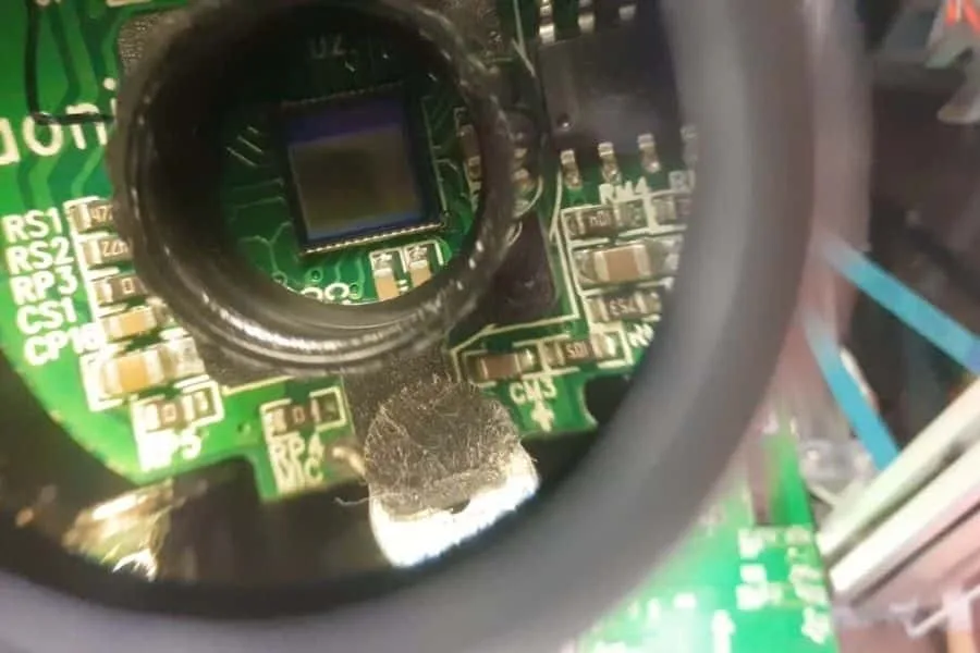
It allows engineers to turn design files into real hardware, validate electrical and mechanical performance, integrate firmware, identify manufacturing problems, and optimize the product before committing to large-scale production.
A reliable PCB Prototype Assembly Service should combine:
Rapid PCB Fabrication + Component Procurement + DFM/DFA + SMT/THT Assembly + AOI/X-Ray + Electrical Testing + Functional Testing
Kingda provides an integrated prototype manufacturing solution with no MOQ, rapid prototyping, advanced SMT capabilities, component procurement, AOI/X-ray inspection, ICT/FCT testing, and prototype-to-volume production support. (GoPCBA)
For startups, OEMs, engineering teams, and product developers, selecting the right Prototype PCB Assembly Manufacturer can reduce development risk, shorten iteration cycles, and create a more efficient transition from prototype to production.