Hardware engineers often approach PCBA procurement as two separate workflows: first PCB fabrication, then component sourcing and assembly. While this model can work, it creates additional supplier handoffs, communication gaps, BOM inconsistencies, and unclear responsibility when problems occur.
A one-stop PCBA service combines these activities into a coordinated manufacturing workflow. Instead of managing PCB fabrication, component procurement, SMT assembly, inspection, and testing through multiple suppliers, the complete process can be managed through one manufacturing partner.
For hardware teams, this approach can simplify project management, reduce avoidable delays, improve traceability, and make it easier to transition from prototype to production.
This guide explains the complete one-stop PCB assembly process, what files engineers should provide, how component sourcing affects production schedules, what inspection and testing should be expected, and how to select a reliable one-stop PCBA manufacturer.
The Seven Stages of a One-Stop PCBA Order
A typical one-stop PCBA manufacturing workflow can be divided into seven major stages.
01 / Design Review
Gerber, BOM, and DFM Review
The first step is a comprehensive review of the customer’s manufacturing data.
A professional engineering team checks the:
- Gerber or ODB++ files
- Bill of Materials (BOM)
- Pick-and-place/Centroid file
- Assembly drawings
- PCB stackup
- Impedance requirements
- Special process requirements
The objective is to confirm that the documents are consistent with one another and that the PCB can be manufactured and assembled reliably.
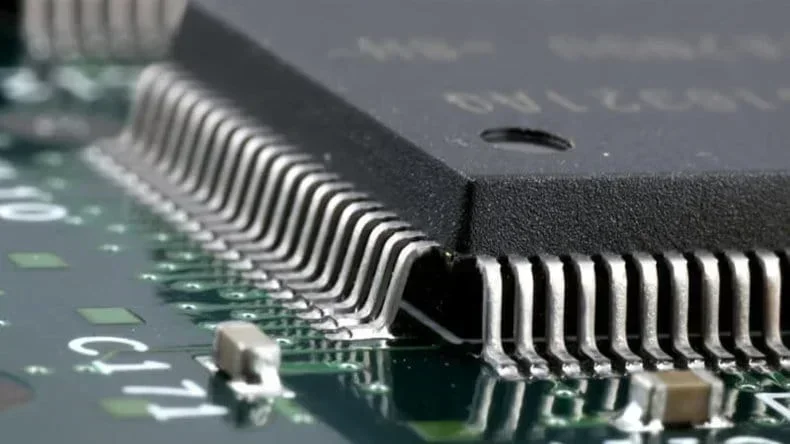
A DFM (Design for Manufacturability) and DFA (Design for Assembly) review can identify problems such as insufficient clearance, incorrect footprints, component placement conflicts, unsupported drill structures, or potential soldering issues before production begins.
Kingda provides engineering support including DFM, DFA, DFX, Gerber review, BOM verification, Pick-and-Place verification, component availability analysis, and manufacturing documentation review. (Kingda)
02 / Component Procurement
BOM Verification and Component Sourcing
Once the design package passes the initial review, the BOM is analyzed against available inventory and supplier channels.
A good one-stop PCB assembly supplier should determine:
- Which components are in stock
- Which parts have long lead times
- Which components are approaching end-of-life
- Which parts require customer approval before substitution
- Which components need special traceability
- Which components require specific date codes or MSL handling
Kingda provides global component procurement and supply-chain management as part of its PCB assembly service, supporting turnkey, partial-kitted, and customer-supplied component models. (Kingda)
03 / PCB Fabrication
Bare PCB Manufacturing
After the PCB design has been approved and materials are confirmed, the bare PCB is manufactured according to the specified construction.
Depending on the product, this may include:
- 2-layer or multilayer PCB
- HDI PCB
- Flexible PCB
- Rigid-flex PCB
- High-frequency PCB
- High-Tg PCB
- Heavy-copper PCB
- Controlled-impedance PCB
Manufacturing quality may include dimensional inspection, impedance verification, AOI and electrical testing according to the product requirements.
Kingda combines PCB fabrication with component procurement and PCB assembly as part of its one-stop PCBA model. (Kingda)
04 / Solder Paste Printing
Precision Solder Paste Application
For SMT production, solder paste is applied to the PCB pads using a precision stencil.
The quality of this stage directly influences subsequent solder-joint reliability.
Important parameters include:
- Stencil thickness
- Aperture dimensions
- Paste type
- Printing pressure
- Printing speed
- Separation speed
- Board alignment
SPI (Solder Paste Inspection) is then used to verify solder-paste volume, height, area, and position before components are mounted.
Kingda’s published SMT capabilities include automated solder paste printing and 3D SPI inspection as part of its SMT production process. (Kingda)
05 / SMT Component Placement
Automated Pick-and-Place Assembly
Once the solder paste has been printed, automated pick-and-place equipment positions components onto the PCB.
Modern SMT equipment uses vision systems to verify:
- Component identity
- Component orientation
- Placement coordinates
- Polarity
- Package position
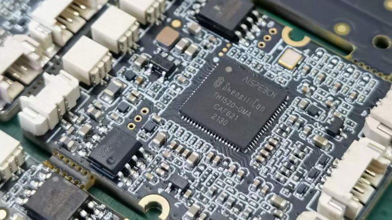
Kingda states that its assembly capabilities support miniature components including 01005 passive components, fine-pitch packages, BGA, QFN, CSP and other high-density components. (Kingda)
06 / Reflow Soldering
Controlled Reflow Process
The populated PCB then passes through a controlled reflow oven.
The temperature profile must be matched to:
- Solder-paste chemistry
- PCB construction
- Component thermal limits
- Lead-free or leaded solder requirements
- Moisture-sensitive components
For lead-free assembly, SAC-type solder processes typically require substantially higher temperatures than traditional SnPb processes.
The reflow profile should therefore be validated rather than simply using a generic oven setting.
07 / Inspection and Testing
AOI, X-Ray, ICT and Functional Testing
The final stage verifies assembly quality and, where required, electrical and functional performance.
Typical inspection methods include:
AOI
Detects:
- Missing components
- Wrong polarity
- Misalignment
- Tombstoning
- Solder bridges
- Visible solder defects
X-Ray Inspection
Particularly useful for:
- BGA
- QFN
- Bottom-terminated components
- Hidden solder joints
ICT
Can verify electrical connections, component characteristics, opens, shorts and other circuit-level conditions when suitable test fixtures are available.
Functional Testing
Tests the assembled PCBA under operating conditions using customer-specific test procedures or fixtures.
Kingda’s published quality workflow includes IQC → SPI → SMT/THT Assembly → AOI → X-Ray → ICT/FCT → OQC, with additional customized testing available according to product requirements. (Kingda)
What Files Should You Provide to a One-Stop PCBA Manufacturer?
A complete manufacturing package is critical to avoiding delays.
Simply sending Gerber files is usually not enough for a professional PCB assembly project.
Gerber Files
The manufacturing data should include:
- Copper layers
- Solder mask
- Silkscreen
- Board outline
- Drill files
- Additional fabrication layers
RS-274X Gerber files remain widely used, while ODB++ and IPC-2581 can provide richer manufacturing information depending on the manufacturing workflow.
Bill of Materials
The BOM should preferably include:
- Reference designator
- Manufacturer
- Manufacturer Part Number (MPN)
- Description
- Quantity
- Package
- Approved alternatives
- DNP information
- Special purchasing requirements
A generic description such as:
100 nF / 0402 / X5R
may not uniquely identify the intended component.
An exact MPN provides significantly clearer procurement information.
Pick-and-Place File
The Centroid file should contain:
- Reference designator
- X coordinate
- Y coordinate
- Rotation
- Layer
- Component information where supported
The origin should correspond correctly with the PCB design data.
Assembly Drawing
Assembly drawings should identify:
- Component orientation
- Pin 1
- Polarity
- Special components
- DNP locations
- Mechanical restrictions
- Special assembly instructions
Stackup and Impedance Specification
For high-speed or RF designs, provide:
- Layer structure
- Dielectric thickness
- Copper thickness
- Target impedance
- Controlled-impedance traces
- Reference planes
This information should be agreed with the PCB manufacturer before fabrication.
BOM and Pick-and-Place Consistency
One of the most important intake checks is ensuring that reference designators are consistent across:
Schematic ↔ PCB Layout ↔ BOM ↔ Pick-and-Place File ↔ Assembly Drawing
A mismatch can lead to wrong-component placement, missing parts, or unnecessary production delays.
Component Sourcing: The Hidden Complexity of One-Stop PCBA
Component sourcing can become the largest schedule constraint in a turnkey PCB assembly project.
PCB fabrication might be completed relatively quickly, but a single unavailable IC can delay the entire order.
Date Code and Traceability
For automotive, medical, aerospace, and other regulated industries, customers may require:
- Lot numbers
- Date codes
- MSL information
- Certificates of Conformance
- Supplier information
- Material traceability
Traceability requirements should be defined before production rather than after delivery.
Kingda states that its production system maintains traceability from incoming materials through final shipment. (Kingda)
Long-Lead-Time Components
Certain semiconductor and specialty electronic components may have extended lead times.
During BOM review, ask:
Which components are currently unavailable, allocated, or subject to extended lead times?
This allows engineers to address procurement risks before PCB fabrication starts.
Approved Alternatives
Not every component can be freely substituted.
Generic passive components may have multiple acceptable alternatives, while specialized components such as:
- RF devices
- MEMS sensors
- precision references
- high-performance processors
- automotive-grade ICs
may require strict manufacturer or part-number control.
Clearly mark these components as No Substitute when necessary.
Reflow Profile and Moisture Management
Engineers sometimes treat reflow soldering as a simple heating process, but it is an important part of PCB assembly reliability.
Lead-Free vs. Leaded Soldering
Specify the solder process clearly.
A typical lead-free process based on SAC solder requires a significantly higher peak temperature than traditional SnPb soldering.
The selected process must be compatible with:
- PCB surface finish
- Component temperature rating
- Solder paste
- Component package
- Assembly requirements
Mixed soldering conditions should be reviewed with the assembler before production.
Moisture-Sensitive Components
Many semiconductor packages carry an MSL (Moisture Sensitivity Level) classification.
Components with higher MSL classifications require controlled storage, baking where necessary, and assembly within their defined floor-life window.
Poor moisture management can cause:
- Package cracking
- Delamination
- Popcorning
- Latent solder-joint reliability problems
For BGA and other moisture-sensitive packages, the manufacturer’s component handling procedures should be confirmed before production.
Inspection and Testing: What Should You Expect?
A professional one-stop PCBA service should provide inspection appropriate to the complexity and risk level of the product.
AOI
Automated Optical Inspection is typically used as a baseline inspection method.
AOI can identify:
- Missing components
- Misalignment
- Wrong polarity
- Tombstoning
- Solder bridges
- Visible solder defects
However, AOI cannot see through a BGA package.
X-Ray Inspection
X-ray inspection can examine hidden solder joints.
It is particularly useful for:
- BGA
- QFN
- LGA
- Bottom-terminated components
- Complex high-density assemblies
For prototype boards containing BGA or QFN packages, X-ray inspection can be valuable even when not contractually mandatory.
ICT
In-Circuit Testing can evaluate electrical connectivity and component-level characteristics when appropriate test fixtures are available.
Functional Testing
Functional testing answers a different question:
Does the completed PCBA actually operate as intended?
The testing procedure may include:
- Power-up
- Communication interfaces
- Sensors
- Displays
- Motors
- Relays
- Data interfaces
- Firmware execution
- Application-specific functions
For functional testing, the customer typically needs to provide the test procedure, expected values, test fixtures or test specifications where applicable.
What Actually Determines PCBA Turnaround Time?
One of the common misconceptions in electronics manufacturing is that PCB fabrication always determines lead time.
For prototype and low-volume orders, component availability can be a larger constraint than PCB fabrication.
For example:
A four-layer PCB may be fabricated quickly, but if one specialized component has a long procurement cycle, that component determines the final delivery date.
How to Reduce PCBA Lead Time
Finalize the BOM Early
Do not wait until the PCB is already fabricated to validate the BOM.
Use Available Components
Where electrically and mechanically appropriate, consider commonly available components.
Approve Alternatives
Pre-approved alternatives can prevent production from stopping because of one unavailable component.
Complete DFM Before Ordering
Early DFM review prevents manufacturing problems from appearing after production has begun.
Coordinate PCB and Component Procurement
A one-stop supplier can synchronize fabrication and component procurement rather than running the two workflows independently.
Kingda’s one-stop model combines PCB manufacturing, component sourcing, SMT/THT assembly, testing and final integration, reducing the number of external handoffs. (Kingda)
One-Stop PCBA vs. Separate PCB and Assembly Suppliers
| Factor | Separate Suppliers | One-Stop PCBA |
|---|---|---|
| PCB Fabrication | Separate supplier | Integrated |
| Component Procurement | Often separate | Integrated |
| PCB Assembly | Separate supplier | Integrated |
| BOM Coordination | Multiple parties | Centralized |
| Engineering Communication | More handoffs | Single technical interface |
| Traceability | May be fragmented | Easier to centralize |
| Quality Responsibility | Shared | More centralized |
| Logistics | Multiple shipments | Consolidated |
| Prototype-to-Production | May require supplier changes | Easier to scale |
The primary advantage is not simply convenience.
The real benefit is process integration.
When PCB fabrication, component procurement and assembly are managed together, it becomes easier to identify the relationship between material availability, PCB construction, assembly requirements and final performance.
Why Choose Kingda for One-Stop PCBA?
Kingda is a one-stop PCB and PCBA manufacturer integrating PCB fabrication, component procurement, SMT, DIP/THT, testing and finished-product assembly. The company states that it supports customers from prototype development through production. (Kingda)
Complete One-Stop Manufacturing
Kingda combines:
PCB Manufacturing → Component Sourcing → SMT → THT/DIP → Inspection → Testing → Box Build
This allows customers to work with one manufacturing partner throughout the product lifecycle. (Kingda)
Engineering and DFM Support
Kingda provides engineering review of:
- BOM
- Gerber files
- Pick-and-place files
- PCB design
- Assembly requirements
- Component availability
This helps identify potential problems before production. (Kingda)
Advanced SMT Capability
Kingda’s published capabilities include:
- 01005 passive components
- Fine-pitch components
- 0.35 mm BGA pitch
- BGA
- QFN
- CSP
- LGA
- PoP
- Double-sided SMT
X-ray, AOI and SPI are integrated into the inspection process. (Kingda)
Comprehensive Quality Control
The published quality workflow includes:
IQC → SPI → SMT/THT → AOI → X-Ray → ICT/FCT → OQC
Kingda also lists FAI, customized testing, IC programming, aging testing, vibration testing and other reliability-testing capabilities. (Kingda)
International Quality Certifications
Kingda states that it has obtained:
- ISO 9001
- ISO 13485
- IATF 16949
- ISO 14001
- UL certification
- IPC membership
These certifications support applications across automotive, medical, industrial automation, AI, communications, energy and other industries. (Kingda)
Production Traceability
Kingda states that its manufacturing system maintains product traceability throughout the production lifecycle, from incoming materials to shipment. (Kingda)
This is especially valuable for products that require strong quality documentation and production-history control.
Conclusion
A one-stop PCBA service is more than a convenient way to order PCB manufacturing and assembly from one supplier.
When implemented correctly, it creates a connected manufacturing workflow:
The quality of this workflow depends heavily on the engineering information provided at the beginning.
A complete BOM, accurate Gerber files, synchronized Pick-and-Place data, clear assembly drawings, explicit impedance requirements, defined component substitutions, and documented testing requirements can significantly reduce manufacturing risk.
At the same time, the right one-stop PCB assembly manufacturer should provide the engineering expertise, supply-chain management, manufacturing capability and quality systems necessary to turn those files into reliable electronic products.
Kingda provides an integrated PCB manufacturing and PCBA solution covering PCB fabrication, component sourcing, SMT/THT assembly, inspection, testing, box build and final product integration. (Kingda)
For hardware teams moving from prototype to production, this integrated model can simplify supplier management while improving manufacturing consistency, traceability and production efficiency.