Almost every modern electronic device relies on a printed circuit board (PCB). From smartphones and laptops to medical equipment, automotive electronics, industrial controllers, telecommunications systems, and AI hardware, PCBs provide both the physical foundation for electronic components and the conductive pathways that connect them.
As electronic products become more sophisticated and development cycles become shorter, engineers increasingly need to validate new designs without waiting several weeks for conventional manufacturing. This has driven the growing demand for quick turn PCB fabrication, a manufacturing approach designed to produce prototype and low-volume PCBs within significantly shorter lead times.
For hardware developers, the value of quick turn PCB manufacturing goes beyond speed. Rapid fabrication allows engineers to identify design problems earlier, complete more iterations, reduce development risk, and transition from prototype to production more efficiently.
This guide explains what quick turn PCB fabrication means, how it works, its major benefits, common challenges, design considerations, and how to select a reliable quick-turn PCB manufacturer.
What Is Quick Turn PCB Fabrication?
Quick turn PCB fabrication refers to the accelerated manufacturing of printed circuit boards using optimized engineering workflows, stocked materials, streamlined production scheduling, and automated manufacturing processes.
While standard PCB production may require several weeks depending on board complexity, quick-turn services are designed to shorten fabrication time to a few days, and in some cases as little as 24–48 hours for suitable standard boards.
The exact turnaround depends on:
- Board layer count
- PCB dimensions
- Material availability
- Trace width and spacing
- Via structures
- Surface finish
- Order quantity
- Controlled-impedance requirements
- HDI or microvia technology
- Testing requirements
- Component availability when assembly is included
The objective is not simply to manufacture faster. A professional quick-turn manufacturer must compress the production cycle while maintaining appropriate PCB quality control, dimensional accuracy, electrical performance, and process consistency.
Why Quick Turn PCB Fabrication Matters
Traditional PCB manufacturing can become a bottleneck during product development. An engineering team may finish a design in a few days but then wait weeks to receive the physical hardware needed for validation.
Quick turn PCB fabrication changes this development cycle.
Instead of:
Design → Wait → Prototype → Test → Wait → Redesign
engineers can move through:
Design → Quick Turn PCB → Test → Modify → Quick Turn PCB → Validate
This shorter feedback loop can significantly accelerate product development.
Faster Time to Market
A shorter PCB manufacturing cycle allows engineering teams to move from concept validation to functional prototypes more quickly.
This is particularly useful for:
- Consumer electronics
- IoT products
- Automotive electronics
- Medical equipment
- Industrial controls
- Communication hardware
- AI hardware
- Robotics
- Aerospace electronics
Faster Design Iteration
A physical prototype often reveals problems that cannot be identified through schematic review alone.
Engineers may discover:
- Thermal hotspots
- EMI problems
- Mechanical interference
- Incorrect component placement
- Signal-integrity issues
- Power-distribution problems
- Unexpected assembly difficulties
With quick turn PCB prototyping, these problems can be corrected and tested again without introducing long manufacturing delays.
Reduced Development Risk
Finding a design problem during prototype development is generally less disruptive than discovering it after mass production has started.
Quick-turn manufacturing enables teams to validate their designs before committing significant production resources.
Lower Overall Development Cost
Quick-turn boards may have a higher unit cost than standard-volume production, but the overall development cost can be lower because engineers can identify and correct problems earlier.
The economic benefit comes from reducing:
- Rework
- Scrap
- Design revisions during mass production
- Production downtime
- Engineering delays
- Product-launch delays
Where Quick Turn PCB Fabrication Is Used
Prototype and Pre-Production
The most common application is rapid production of prototypes.
Engineers can use fast PCB fabrication to validate:
- Circuit functionality
- Component placement
- Signal integrity
- Mechanical fit
- Thermal performance
- Assembly feasibility
Design Modifications
When an existing PCB requires a design change, quick-turn manufacturing allows the revised version to be built quickly for comparison and testing.
Pilot Production
Quick-turn PCB services can also support limited production runs before full-scale manufacturing.
This allows manufacturers to validate:
- Assembly processes
- Component sourcing
- Production fixtures
- Test procedures
- Manufacturing yield
Failure Analysis and Replacement Boards
When a product experiences a PCB-related failure, rapid PCB fabrication can provide replacement boards for troubleshooting and field validation.
Urgent Supply Requirements
Quick-turn manufacturing can also help companies respond to:
- Unexpected PCB shortages
- Production disruptions
- Engineering changes
- Customer-specific requirements
- Urgent replacement orders
How Quick Turn PCB Manufacturing Works
The quick turn PCB manufacturing process follows the same fundamental manufacturing principles as standard PCB production, but the workflow is optimized for speed.
Step 1: Engineering Review and DFM
The process begins with the customer’s manufacturing data.
Typical files include:
- Gerber files
- ODB++
- IPC-2581
- NC drill files
- PCB fabrication drawings
- Stackup specifications
Engineers perform a DFM (Design for Manufacturability) review to identify potential production problems before fabrication begins.
Important checks include:
- Trace width
- Trace spacing
- Hole sizes
- Annular ring
- Copper-to-edge clearance
- Solder-mask clearance
- Layer registration
- Via structures
- Board thickness
- Material availability
The earlier these issues are identified, the easier it is to maintain the required quick-turn schedule.
Step 2: Material Selection and Preparation
Quick-turn manufacturers typically keep commonly used materials in stock.
Common choices include:
Standard FR-4
Suitable for most general-purpose electronic products.
High-TG FR-4
Used for applications requiring improved thermal performance and dimensional stability.
High-Frequency Laminates
Used in RF, microwave, 5G, radar, and high-speed applications.
Aluminum PCB Materials
Suitable for applications requiring effective thermal dissipation, such as LED lighting and power electronics.
Using materials that are already available is one of the simplest ways to shorten manufacturing lead time.
Step 3: Inner-Layer Imaging
For multilayer boards, inner copper layers are produced using precision imaging technology.
Modern PCB fabrication facilities commonly use Laser Direct Imaging (LDI) to achieve accurate circuit patterns and layer registration.
Step 4: Lamination
Inner-layer cores, prepreg, and copper foil are stacked according to the approved PCB stackup.
The stack is then laminated under controlled heat and pressure.
For quick-turn production, stable materials and standardized stackups help reduce setup and process time.
Step 5: Drilling
CNC mechanical drilling creates through-holes and plated-hole structures.
For advanced HDI boards, laser drilling may be used to create microvias.
The drilling method depends on:
- Hole diameter
- Board thickness
- Layer structure
- Via technology
- HDI requirements
Step 6: Copper Plating
The drilled holes are cleaned and chemically prepared before copper deposition.
Electroless copper provides an initial conductive layer, followed by electrolytic copper plating to build the required copper thickness.
Step 7: Outer-Layer Imaging and Etching
Outer-layer circuitry is created using precision imaging, copper plating, and etching processes.
The result is the finished:
- Signal traces
- Pads
- Ground planes
- Power planes
- Plated holes
Step 8: Solder Mask and Surface Finish
The PCB receives a solder mask to protect the copper circuitry.
Depending on the application, manufacturers may use:
- HASL
- Lead-free HASL
- ENIG
- OSP
- Immersion Silver
- ENEPIG
The appropriate finish depends on assembly method, cost, reliability, solderability, and component requirements.
Step 9: Electrical Testing and Inspection
Before shipment, quick-turn PCBs should still undergo appropriate quality checks.
These may include:
- Electrical continuity testing
- Flying-probe testing
- AOI
- Dimensional inspection
- Visual inspection
- Impedance testing where required
Speed should never be achieved by simply eliminating critical quality-control procedures.
Design Considerations for Quick Turn PCB Fabrication
A design intended for rapid production should be designed around the manufacturer’s actual capabilities.
Use Standard Materials
Standard FR-4 and commonly stocked copper weights can usually be produced faster than specialized laminates.
Use Standard Layer Counts
Two-layer and four-layer boards are typically easier to manufacture quickly than highly complex multilayer boards.
Every additional layer can introduce:
- Additional lamination
- Longer drilling cycles
- More registration requirements
- Greater process complexity
Avoid Unnecessary Advanced Features
Features such as:
- Microvias
- Blind vias
- Buried vias
- Extremely small traces
- Heavy copper
- Advanced surface finishes
can increase both cost and lead time.
They should be used when required by the application rather than simply because the manufacturing technology is available.
Submit Complete Manufacturing Files
Incomplete or inconsistent files are a major cause of avoidable delays.
Before submitting a quick-turn order, verify:
- Gerber layers
- NC drill files
- Board outline
- Stackup
- Material
- Surface finish
- Copper thickness
- Impedance requirements
Perform DFM Before Ordering
A pre-production DFM review can identify potential issues before the board enters fabrication.
This is one of the most effective ways to protect a quick-turn schedule.
Quick Turn PCB Fabrication vs Standard PCB Manufacturing
| Factor | Quick Turn PCB | Standard PCB Manufacturing |
|---|---|---|
| Lead Time | Typically days | Typically longer |
| Order Quantity | Prototype to low volume | Medium to high volume |
| Unit Cost | Higher for small quantities | Lower at volume |
| Engineering Flexibility | High | Moderate |
| Material Selection | Often based on stocked materials | Broader material choices |
| Best Application | Prototypes, urgent builds, pilot runs | Planned production |
| Design Changes | Easier to accommodate | Less flexible after production starts |
| Production Strategy | Speed-focused | Cost and volume-focused |
The fundamental trade-off is speed versus production economics.
Quick-turn manufacturing is usually most valuable when schedule risk is more expensive than the premium paid for accelerated production.
When Quick Turn PCB Fabrication May Not Be Practical
Not every PCB can realistically be produced within 24–72 hours.
Rapid manufacturing may be difficult when a project requires:
Highly Complex HDI Structures
Advanced sequential lamination, stacked microvias, and extremely fine features require more processing time.
Special Materials
Exotic or low-volume materials may need to be ordered before fabrication can begin.
Long-Lead Components
For PCBA projects, the PCB itself may be produced quickly while component procurement becomes the real schedule constraint.
Very Large Quantities
Manufacturing hundreds of thousands or millions of boards generally requires a different production strategy based on capacity, panel utilization, automation, and production scheduling.
Extensive Testing
Certain medical, aerospace, automotive, or industrial products may require additional electrical, environmental, mechanical, or functional testing.
Challenges in Quick Turn PCB Manufacturing
DFM Constraints
The design must fall within the manufacturing capability of the chosen factory.
The fastest production is usually achieved when engineers work with the manufacturer early rather than submitting highly complex designs and expecting the factory to solve manufacturability problems afterward.
Component Availability
For quick turn PCB assembly, component sourcing can become more important than PCB fabrication.
One unavailable component can delay the entire PCBA project.
For turnkey assembly, engineers should review:
- Component stock
- Manufacturer part numbers
- Lifecycle status
- Lead times
- Approved substitutes
Testing Requirements
Fast manufacturing should not mean eliminating necessary testing.
The test strategy should be based on product risk.
For example:
- Basic prototypes may require visual inspection and electrical continuity testing.
- BGA assemblies may require X-ray.
- High-reliability products may require ICT and functional testing.
Quality Control
Automation helps maintain consistency during rapid production.
Modern quick-turn facilities can combine:
SPI + AOI + X-ray + Electrical Testing + Functional Testing
to maintain quality while reducing manual inspection time.
How to Overcome Quick Turn PCB Manufacturing Challenges
Design for Speed
Use manufacturer-approved design rules from the beginning.
Standardize Materials
Common materials and standard stackups are generally easier to process rapidly.
Pre-Approve Alternative Components
For PCB assembly projects, pre-approved substitutes can reduce procurement delays.
Use Modular Hardware Architectures
Complex products can sometimes be divided into smaller PCB modules, allowing multiple boards to be manufactured or tested in parallel.
Prioritize Critical Tests
Identify which electrical, thermal, mechanical, and functional parameters directly determine product performance.
This enables the manufacturer to build a test strategy that protects quality without unnecessarily extending lead time.
Kingda Quick Turn PCB Fabrication and Assembly
Kingda provides integrated PCB fabrication and PCBA manufacturing services, supporting projects from rapid prototypes through production.
Its one-stop manufacturing model combines:
PCB Design Support → PCB Fabrication → Component Procurement → SMT Assembly → THT Assembly → Inspection → Testing
This approach reduces the need to coordinate multiple suppliers and can improve communication between engineering, procurement, PCB fabrication, and assembly teams.
Rapid PCB Prototyping
Kingda’s published rapid PCBA prototype capabilities support:
- Small-batch production
- Quick-turn PCB assembly
- SMT assembly
- Through-hole assembly
- Mixed-technology assembly
- BGA and QFN packages
- 01005 and 0201 components
- Functional testing
- AOI and X-ray inspection
Kingda states that prototype PCBA can be produced with flexible quantities and rapid lead times depending on project specifications and component availability.
Broad PCB Manufacturing Capabilities
Kingda supports a range of PCB technologies, including:
- Multilayer PCB
- HDI PCB
- High-frequency PCB
- High-TG PCB
- Heavy-copper PCB
- Rigid-flex PCB
- Metal-core PCB
- Impedance-controlled PCB
- Blind and buried via PCB
- High-density PCB
This provides engineers with a pathway from conventional prototypes to more advanced production technologies.
Engineering and DFM Support
Kingda’s engineering services include:
- DFM review
- DFA analysis
- BOM verification
- Gerber review
- Pick-and-place file verification
- Component availability analysis
- Alternative component recommendations
- Manufacturing optimization
This engineering support helps reduce design-related delays before production starts.
Advanced Quality Control
Kingda’s published PCBA capabilities include:
- SPI
- AOI
- X-ray inspection
- ICT
- FCT
- FAI
- Functional testing
These inspection and testing technologies help maintain production consistency for prototype and volume PCBA projects.
Quality Certifications
Kingda states that its quality management system includes:
- ISO 9001
- ISO 13485
- IATF 16949
- ISO 14001
- UL certification
- IPC membership
These certifications support applications including automotive, medical, industrial, telecommunications, power electronics, and other reliability-sensitive electronics sectors.
When Should You Choose Quick Turn PCB Fabrication?
Quick turn PCB fabrication is particularly valuable when:
- A prototype is required urgently.
- Engineers need multiple design iterations.
- A product launch deadline is approaching.
- A failed PCB needs to be replaced quickly.
- A pilot production run is required.
- A customer needs engineering samples.
- Production has been interrupted by a PCB shortage.
- Hardware and firmware teams need physical boards for development.
For large, stable production volumes with predictable schedules, conventional PCB manufacturing is usually more economical.
How to Reduce Quick Turn PCB Cost
Rapid production does not automatically have to be expensive.
Several strategies can reduce total cost.
Use Standard Board Structures
Choose standard layer counts and materials whenever the application allows.
Optimize Panelization
Efficient panel utilization reduces material waste and can improve machine utilization.
Consolidate Orders
Combining several small builds may reduce setup and tooling costs.
Prepare Complete Documentation
Accurate Gerber, BOM, stackup, and fabrication drawings reduce engineering clarification time.
Check Component Availability Before Assembly
For turnkey PCBA, verify component stock before committing to a production schedule.
Conclusion
Quick turn PCB fabrication has become an important manufacturing strategy for modern electronics development. By combining accelerated engineering review, stocked materials, streamlined fabrication, automated inspection, and efficient production scheduling, manufacturers can compress PCB development cycles from weeks into days for suitable designs.
The greatest value of quick-turn manufacturing is not simply faster delivery. It creates a shorter engineering feedback loop that allows teams to:
Design → Build → Test → Improve → Validate
This makes product development more flexible, reduces technical risk, and can accelerate time-to-market.
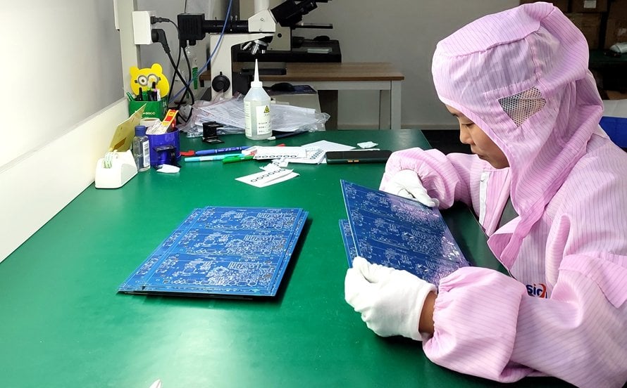
However, successful quick turn PCB manufacturing requires more than simply placing a rush order. Designers must consider DFM, material availability, board complexity, component sourcing, testing requirements, and manufacturing capabilities from the beginning.
Kingda combines quick-turn PCB fabrication, PCB assembly, component sourcing, engineering support, AOI, X-ray, ICT and functional testing in an integrated manufacturing model, helping customers move from PCB prototype to production with fewer supplier handoffs and better process coordination.
For engineering teams that need fast prototypes without sacrificing manufacturing discipline, a properly managed quick turn PCB fabrication process can provide a significant advantage in today’s rapidly changing electronics market.