Modern electronic products are becoming increasingly compact, intelligent, and powerful. Technologies such as artificial intelligence, IoT, wireless communication, automotive electronics, medical electronics, and industrial automation are driving continuous innovation across the electronics industry.
Behind these advanced products is a carefully controlled PCB assembly process. A bare printed circuit board provides the electrical foundation, but the board cannot perform its intended function until electronic components are mounted, soldered, inspected, and tested.
At first glance, PCB assembly may appear relatively straightforward because it mainly involves SMT assembly and PTH/THT assembly. In practice, however, a reliable PCBA manufacturing process contains many supporting engineering, inspection, testing, material-control, and quality-assurance operations.
A complete PCB assembly workflow may include file review, DFM/DFA analysis, stencil preparation, solder paste printing, component placement, reflow soldering, AOI inspection, X-ray inspection, PTH assembly, functional testing, final quality inspection, labeling, and packaging.
This guide provides a detailed explanation of the PCB assembly process, including the major manufacturing stages, key quality controls, common assembly technologies, and how Kingda supports customers from prototype to volume production.
Step 1: Prepare the Files Required for PCB Assembly
The first and one of the most important stages of the PCB assembly process is preparing and reviewing all manufacturing and assembly data.
A complete PCB assembly package normally includes:
- Gerber files
- BOM (Bill of Materials)
- Pick-and-Place/Centroid files
- Assembly drawings
- PCB schematics
- PCB stack-up information
- Special process instructions
- Testing requirements
- Programming or firmware requirements
Gerber Files
Gerber files describe the physical structure of the PCB, including copper layers, solder mask, silkscreen, and board outlines.
They are used during engineering review and help the manufacturer verify whether the PCB layout is compatible with the intended PCB assembly process.
For example, the CAM engineer may identify inconsistencies between component footprints and PCB pads. A component package may be larger or smaller than the actual pad geometry, which can create soldering or placement problems.
BOM Verification
The BOM (Bill of Materials) provides detailed information about every component required for assembly.
A professional BOM should include:
- Reference designator
- Manufacturer name
- Manufacturer Part Number (MPN)
- Component description
- Package type
- Quantity
- Approved alternatives
- DNP information
- Special component requirements
BOM accuracy is critical because even a single incorrect MPN can result in the wrong component being installed.
Pick-and-Place File
The Pick-and-Place file, also called the Centroid file, contains the X/Y coordinates, component reference designators, rotation angles, and PCB side information required by automated SMT machines.
The consistency between the BOM and Pick-and-Place file is particularly important. Any mismatch can cause incorrect component placement.
Additional Manufacturing Data
Customers may also provide:
- Assembly drawings
- Schematic diagrams
- 3D PCB models
- Product drawings
- Test procedures
- Programming instructions
These files may not always be mandatory, but they can significantly improve engineering communication and production accuracy.
DFM and DFA Review for PCB Assembly
Before production begins, manufacturers should perform DFM (Design for Manufacturability) and DFA (Design for Assembly) analysis.
The purpose is to identify design problems before they become manufacturing problems.
Typical issues include:
- Incorrect component footprints
- BOM and layout mismatches
- Incorrect component quantities
- Insufficient component spacing
- Wrong polarity
- Obsolete components
- Difficult-to-source components
- Inappropriate solder-pad dimensions
- Assembly clearance problems
A professional engineering review can significantly reduce production delays and rework.
Kingda provides DFM/DFA review, BOM verification, Gerber analysis, Pick-and-Place verification, and engineering support before production. This helps customers identify design and manufacturing risks early in the project.
Generate the Production Process File
After engineering questions are resolved, the manufacturer creates a detailed manufacturing process document or production traveler.
Depending on the project, this document may define:
- IQC requirements
- Solder paste type
- Stencil specifications
- SMT placement parameters
- Reflow profile
- PTH assembly requirements
- Selective or wave soldering conditions
- Conformal coating
- Dispensing
- Programming
- Functional testing
- Final inspection
- Packaging requirements
This process documentation ensures that every production department follows the same approved manufacturing instructions.
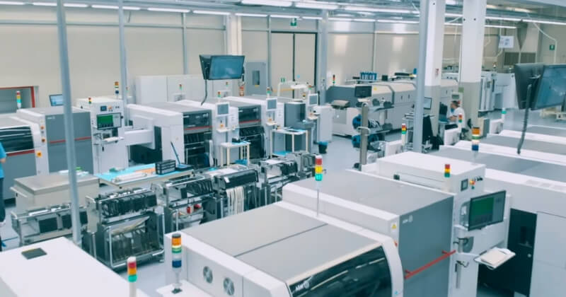
Step 2: SMT PCB Assembly
Once all documentation, materials, and tools are ready, the SMT PCB assembly process can begin.
SMT (Surface Mount Technology) is the dominant assembly technology used in modern electronics because it supports miniaturized components, high component density, and automated production.
The major SMT stages include:
Stencil Preparation → Solder Paste Printing → SPI → Component Placement → First Article Inspection → Reflow → AOI → Testing
Prepare the SMT Stencil
An SMT stencil is used to deposit solder paste onto PCB pads.
Modern stencils are commonly manufactured using precision laser cutting followed by polishing to achieve smooth aperture walls.
Stencil thickness depends on:
- PCB design
- Component package
- Pad geometry
- Required solder volume
- Fine-pitch requirements
A poorly designed stencil can lead to solder bridging, insufficient solder, component misalignment, and other assembly defects.
Kingda supports customized stencil and fixture preparation according to PCB design and assembly requirements.
Generate Pick-and-Place Data
The SMT production line requires accurate Pick-and-Place data.
The placement system uses this information to determine:
- Component location
- Component rotation
- PCB side
- Component type
- Placement sequence
Accurate data helps improve placement speed and repeatability.
Prepare Assembly Fixtures and Support Tools
Some PCB designs require special support tooling.
For example:
- Flexible PCBs
- Rigid-flex PCBs
- Thin PCBs
- Boards with edge-sensitive components
- Single PCBs with components close to the board edge
These boards may require custom carriers or support fixtures to prevent warpage and movement during printing and placement.
This is particularly important for flex PCB assembly because flexible substrates may deform when subjected to printing and component-placement forces.
Solder Paste Printing
The next step is solder paste printing.
The PCB is aligned with the stencil, and solder paste is forced through the stencil apertures using a squeegee.
The quality of the solder paste printing process directly affects solder-joint reliability.
Important parameters include:
- Solder paste volume
- Stencil thickness
- Aperture geometry
- Printing speed
- Squeegee pressure
- PCB support
- Stencil alignment
For lead-free production, SAC-based solder alloys are commonly used.
Proper solder paste storage is also important. Solder paste should be stored according to the manufacturer’s temperature and handling recommendations and should reach the required working temperature before printing.
Solder Paste Inspection
After printing, SPI (Solder Paste Inspection) checks the deposited solder paste.
SPI can identify:
- Insufficient solder
- Excessive solder
- Offset solder deposits
- Missing paste
- Abnormal paste height
- Abnormal solder volume
Early detection prevents defects from continuing to the placement and reflow stages.
Component Placement
After solder paste printing, components are placed onto the PCB using high-speed pick-and-place machines.
The equipment uses vision systems to verify PCB fiducials and component orientation.
Modern SMT lines can handle a wide range of components, including:
- 0201
- 01005
- QFN
- QFP
- BGA
- Fine-pitch ICs
- Connectors
- Power components
Kingda’s published SMT capabilities include automated high-speed placement and support for miniaturized and fine-pitch components, making it suitable for prototype, low-volume, and volume-production applications.
In-Process Quality Control
IPQC (In-Process Quality Control) plays an important role during SMT assembly.
Operators and quality engineers continuously monitor:
- Solder paste quality
- Component placement accuracy
- Feeder setup
- Component identity
- Machine parameters
- Reels and material changes
This helps prevent incorrect components from entering the production batch.
First Article Inspection
Before running the complete production batch, many PCB assembly projects require FAI (First Article Inspection).
The first assembled PCB is inspected to verify:
- Correct components
- Correct orientations
- Correct placement
- Soldering quality
- BOM consistency
- Assembly drawing compliance
First article inspection is particularly important for new products, engineering changes, and new manufacturing programs.
Reflow Soldering
After component placement, the PCB enters the reflow soldering process.
The solder paste is heated according to a carefully controlled thermal profile until it melts and forms permanent electrical and mechanical connections.
A typical thermal profile consists of:
Preheat → Soak → Reflow → Cooling
The exact profile depends on:
- Solder alloy
- PCB materials
- Component thermal limits
- Board thickness
- Copper density
- Component distribution
Proper thermal control helps prevent:
- Cold solder joints
- Tombstoning
- Voiding
- Bridging
- Component damage
- PCB warpage
AOI Inspection
After reflow, AOI (Automated Optical Inspection) is performed.
AOI uses high-resolution cameras and software algorithms to identify:
- Missing components
- Wrong component placement
- Incorrect polarity
- Component displacement
- Solder bridges
- Tombstoning
- Visible solder defects
Kingda integrates automated inspection into its production workflow to improve manufacturing consistency and defect detection.
In-Circuit Testing
ICT (In-Circuit Testing) is an electrical test method designed to identify PCB assembly defects.
ICT may test:
- Resistance
- Capacitance
- Inductance
- Continuity
- Voltage
- Open circuits
- Short circuits
- Component presence
- Incorrect polarity
ICT normally requires a dedicated fixture designed for the specific PCB.
Although ICT cannot necessarily test every function of a complex PCB, it can identify many manufacturing defects efficiently.
X-Ray Inspection for BGA and Hidden Solder Joints
AOI and visual inspection cannot directly inspect solder joints hidden underneath packages such as:
- BGA
- QFN
- LGA
- CSP
For these components, X-ray inspection provides internal visibility.
X-ray inspection can identify:
- Solder voids
- Open joints
- Bridging
- Insufficient solder
- Misalignment
- Poor solder connections
For complex prototype and high-reliability PCB assemblies, X-ray inspection is particularly valuable.
Visual Inspection and QA Check
Even with automated inspection, experienced quality engineers remain important.
A final visual inspection can identify issues that automated systems may not fully classify, including:
- Surface contamination
- Mechanical damage
- Labeling problems
- Connector defects
- Cosmetic defects
- Unusual solder conditions
After all inspections and testing have been completed, QA (Quality Assurance) performs the final batch review.
Depending on customer requirements and product risk, this may include random sampling or 100% final inspection.
Step 3: PTH / THT PCB Assembly
PTH assembly, also known as THT assembly, is another important PCB assembly technology.
Through-hole components have leads that pass through drilled holes in the PCB.
Typical PTH components include:
- Connectors
- Transformers
- Relays
- Large capacitors
- Power components
- Switches
The typical THT/PTH workflow is:
Tooling Preparation → Component Insertion → Wave/Selective Soldering → Lead Cutting → Inspection
Prepare Tooling Fixtures
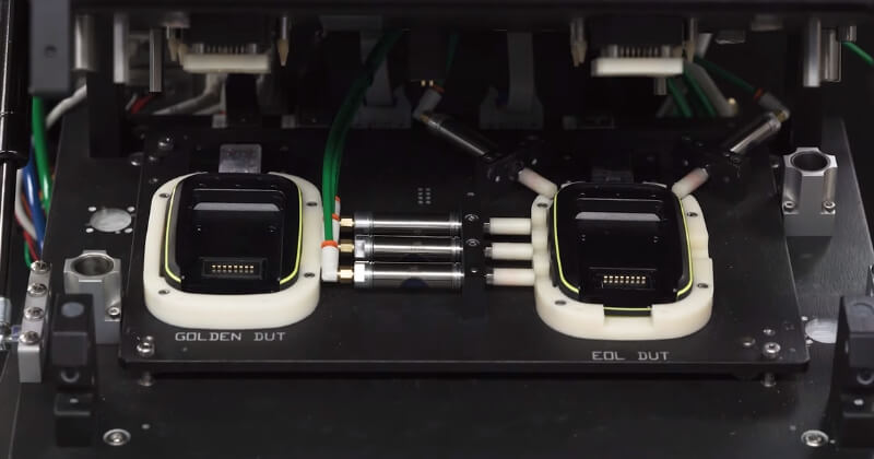
Tooling fixtures support the PCB during through-hole soldering.
They can:
- Protect SMT components
- Support heavy components
- Prevent PCB deformation
- Mask selected areas during soldering
Fixtures are especially important when boards contain both SMT and PTH components.
Insert Through-Hole Components
Components can be inserted manually or automatically.
Manual insertion is common for:
- Prototypes
- Small-volume production
- Customized assemblies
- Irregular components
Automated insertion is more suitable for standardized high-volume products.
Wave Soldering
During wave soldering, molten solder forms a controlled wave beneath the PCB.
As the PCB moves across the wave, the solder wets the exposed through-hole leads and creates permanent solder joints.
Wave soldering is highly efficient for larger volumes of THT assembly.
Selective Soldering
For mixed-technology boards, selective soldering is often preferred.
It allows the manufacturer to solder specific through-hole joints without exposing the entire underside of the PCB to molten solder.
This reduces thermal impact on nearby SMT components.
Lead Cutting
After soldering, excess component leads may be trimmed.
Automated lead-cutting equipment can improve production speed and consistency during larger-volume THT assembly.
PTH Quality Inspection
The completed PTH assembly is inspected for:
- Missing components
- Incorrect components
- Cold solder joints
- Insufficient solder
- Solder bridges
- Mechanical damage
- Excess lead length
Step 4: Manual PCB Assembly
Not every component or manufacturing operation can be economically automated.
Manual PCB assembly may still be required for:
- Prototypes
- Small batches
- Rare components
- Mechanical parts
- Engineering modifications
- Rework
- Repair
Manual soldering quality depends heavily on operator training and process control.
Professional manufacturers should use controlled soldering equipment and maintain appropriate operator qualification and inspection procedures.
Kingda supports manual assembly and specialized rework where required by product design.
Step 5: Functional Testing
Once the components have been completely assembled, the PCB may undergo functional testing (FCT).
Functional testing verifies the actual behavior of the assembled board under operating conditions.
Depending on the product, the test may include:
- Power-on testing
- Voltage and current testing
- Sensor verification
- Communication interfaces
- Display operation
- Motor operation
- RF communication
- Programming verification
- Firmware execution
Testing fixtures may be supplied by the customer or developed according to approved test procedures.
For complex products, functional testing can be one of the most important steps in confirming that the PCBA performs correctly.
Step 6: FQC — Final Quality Control
FQC (Final Quality Control) is the final quality gate before shipment.
The final inspection may verify:
- Component completeness
- Soldering quality
- PCB appearance
- Labels
- Connectors
- Functional-test results
- Packaging requirements
- Customer specifications
Only assemblies that meet the approved quality criteria should be released for shipment.
Step 7: Labeling and Traceability
Many electronic products require product identification or traceability marks.
These may include:
- Part numbers
- Serial numbers
- QR codes
- Barcodes
- Revision numbers
- Production dates
- Customer-specific labels
Laser marking can also be used for permanent identification.
Proper PCB assembly traceability helps manufacturers and customers track production history, simplify after-sales service, and improve root-cause analysis when quality issues occur.
Step 8: PCB Assembly Packaging
Packaging is the final stage of the PCB assembly process, but it should not be underestimated.
Electronic assemblies must be protected against:
- Electrostatic discharge
- Mechanical shock
- Humidity
- Dust
- Vibration
Typical packaging methods include:
- ESD-safe bags
- Moisture barrier bags
- Bubble protection
- Foam inserts
- Anti-static trays
- Reinforced cartons
For overseas shipping, packaging must be designed to withstand the transportation environment and protect boards throughout the logistics process.
Complete PCB Assembly Process Flow
For a typical SMT + THT project, the complete workflow can be summarized as:
Design Data Review → DFM/DFA → BOM Verification → Production File Preparation → SMT Stencil → Solder Paste Printing → SPI → Component Placement → FAI → Reflow Soldering → AOI → THT/PTH Assembly → Wave/Selective Soldering → X-Ray/ICT → Functional Testing → FQC → Labeling → Packaging → Shipment
This workflow can be adapted according to product complexity, technology, volume, testing requirements, and customer specifications.
How to Improve PCB Assembly Quality
A stable PCBA manufacturing process depends on coordinated control across engineering, materials, production, and testing.
Improve BOM Accuracy
Ensure all manufacturer part numbers, quantities, package types, and approved substitutions are correct before production.
Perform DFM/DFA Early
Identify footprint, spacing, polarity, solderability, and assembly issues before purchasing components or producing the first batch.
Control Solder Paste
Proper solder-paste storage, preparation, printing, and SPI inspection are essential to achieving stable SMT soldering.
Monitor Reflow Profiles
Each PCB should be processed using a thermal profile appropriate for its solder alloy, board structure, and component limits.
Use Multiple Inspection Methods
SPI, AOI, X-ray, ICT, and FCT each detect different categories of defects. Combining the appropriate methods produces more comprehensive quality coverage.
Maintain Traceability
Link components, lots, production records, inspection results, and test data to the finished assembly whenever traceability is required.
Why Choose Kingda for PCB Assembly?
Kingda provides integrated PCB assembly services covering PCB fabrication, component sourcing, SMT, THT, inspection, testing, and system-level assembly.
The company is positioned to support projects ranging from engineering prototypes to volume production.
One-Stop PCB and PCBA Manufacturing
Kingda integrates:
PCB Fabrication → Component Procurement → SMT Assembly → THT Assembly → Testing → Final Assembly
This one-stop structure reduces the need for customers to coordinate separate PCB, component, and assembly suppliers.
Advanced SMT Production
Kingda’s published capabilities include automated SMT assembly for fine-pitch and miniature components, including 01005, 0201, BGA, QFN, and other complex packages.
The company also supports advanced inspection equipment such as SPI, AOI, and X-ray.
Comprehensive Testing
Kingda supports multiple testing methods, including:
- AOI
- X-ray
- FAI
- ICT
- FCT
- Customized functional testing
This allows inspection strategies to be matched to the requirements and risk level of each product.
Flexible Production Capability
Kingda supports:
- PCB prototypes
- Low-volume production
- Medium-volume production
- High-volume PCB assembly
- Mixed SMT/THT production
This enables customers to continue working with one manufacturing partner as products move from prototype to production.
Engineering and DFM Support
Kingda provides engineering assistance with:
- DFM
- DFA
- BOM verification
- Component sourcing
- Manufacturing file review
- Assembly optimization
- Production troubleshooting
This engineering involvement helps identify problems before they become production issues.
Quality Certifications
According to Kingda’s published company information, its quality management system includes ISO 9001, ISO 13485, IATF 16949, ISO 14001, and UL certification, with capabilities supporting automotive, medical, industrial, and other demanding applications.
Component Sourcing and Traceability
Kingda also provides component procurement and supply-chain support, helping customers manage component availability, sourcing risks, and production traceability.
Conclusion
The PCB assembly process is much more than simply mounting electronic components onto a circuit board.
A professional PCB assembly manufacturer must coordinate engineering review, BOM verification, stencil preparation, solder paste printing, SMT placement, reflow soldering, THT assembly, AOI, X-ray, ICT, functional testing, final quality control, traceability, and packaging.
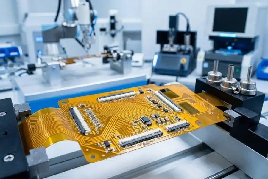
SMT provides high-density and highly automated assembly for modern electronics, while THT remains valuable for mechanically robust and high-power components. Combining SMT and THT enables manufacturers to support complex mixed-technology products.
For engineers and product developers, the most important factors are not only equipment and production capacity, but also DFM/DFA engineering, material management, process control, inspection capability, component sourcing, and traceability.
Kingda’s one-stop manufacturing model integrates PCB fabrication, component procurement, SMT/THT assembly, testing, and final product integration, helping customers simplify the supply chain and move efficiently from prototype to mass production.