As electronic products become increasingly connected and intelligent, technologies such as wireless communication, artificial intelligence (AI), high-speed computing, and big-data processing are driving higher requirements for electronic manufacturing. At the center of many of these systems are printed circuit boards (PCBs), which provide the electrical and mechanical platform for electronic components.
For conventional consumer electronics, basic PCB assembly processes may be sufficient. However, products used in aerospace, automotive, medical, industrial, telecommunications, and defense applications often operate under demanding environmental and electrical conditions. In these applications, a PCB failure can result in equipment downtime, expensive repairs, or serious safety consequences.
This is why high-reliability PCB assembly requires more than simply mounting components and soldering them to a board. It involves controlled materials, robust PCB design, precise assembly processes, rigorous inspection, reliability testing, traceability, and continuous process control.
This guide explains what high-reliability PCB assembly is, how it works, which materials and processes are important, common reliability risks, and how to choose a capable high-reliability PCB assembly manufacturer.
What Is High-Reliability PCB Assembly?
High-reliability PCB assembly is a controlled electronics manufacturing process designed to produce assembled circuit boards that maintain stable electrical and mechanical performance over an extended operating life and under demanding environmental conditions.
Compared with standard PCB assembly, high-reliability assembly places greater emphasis on:
- Material quality and consistency
- Design for reliability
- Process control
- Cleanliness
- Thermal management
- Solder-joint integrity
- Electrical testing
- Environmental and mechanical reliability
- Traceability
- Qualification and documentation
These requirements are particularly important for products exposed to:
- High or low temperatures
- Humidity and moisture
- Vibration and mechanical shock
- Thermal cycling
- Electrical overstress
- Chemical contamination
- Long operating periods
- Safety-critical applications
Typical applications include automotive electronics, medical devices, aerospace systems, industrial controls, telecommunications equipment, power electronics, and defense electronics.
What Makes a PCB Assembly High Reliability?
High reliability is not created by a single manufacturing step. It results from the interaction of design, materials, process control, inspection, and testing.
High-Quality Materials
Reliable PCB assemblies begin with materials selected according to the application’s environmental and electrical requirements.
Common examples include:
- High-Tg FR-4 laminates
- Low-loss high-frequency materials
- Polyimide for flexible circuits
- Heavy-copper PCB materials
- High-reliability solder alloys
- Controlled-quality solder paste
- Robust surface finishes
The material system must be compatible with the assembly temperature profile and the product’s expected operating environment.
Reliability-Oriented PCB Design
PCB design has a major influence on long-term reliability.
Designers should evaluate:
- Trace width and spacing
- Copper thickness
- Via structures
- Thermal paths
- Component derating
- Creepage and clearance
- Controlled impedance
- Power distribution
- Mechanical stress
- Component placement
- Board-level thermal expansion
For high-density applications, HDI PCB technology, microvias, controlled impedance, and advanced stackups may be required.
Comprehensive Reliability Testing
High-reliability products typically require more testing than standard commercial electronics.
Depending on the application, testing may include:
- Thermal cycling
- High-temperature storage
- Humidity testing
- Burn-in
- Power cycling
- Mechanical vibration
- Mechanical shock
- Electrical stress testing
- Insulation resistance testing
- Functional testing
The exact test program should be established according to product requirements, risk level, customer specifications, and applicable industry standards.
Types of PCB Assembly
PCB assembly can be classified according to both the number of assembled sides and the mounting technology.
Single-Sided PCB Assembly
Components are mounted on one side of the PCB.
Advantages include:
- Lower assembly cost
- Simpler manufacturing
- Easier inspection
- Suitable for relatively simple circuits
Typical applications include:
- Simple controllers
- Indicators
- Basic consumer electronics
- Low-density industrial boards
Double-Sided PCB Assembly
Components are mounted on both sides of the PCB.
Double-sided assembly provides:
- Higher component density
- Better space utilization
- More flexible routing
- Greater system functionality
It is widely used in modern electronic devices where board size and component density are important.
SMT Assembly
Surface Mount Technology (SMT) mounts components directly onto PCB pads.
SMT is the dominant assembly technology for modern electronics because it supports:
- Miniaturized components
- High component density
- Automated production
- High placement accuracy
- High-speed manufacturing
Common SMT components include:
- Resistors
- Capacitors
- Diodes
- MOSFETs
- ICs
- QFNs
- BGAs
- CSPs
THT Assembly
Through-Hole Technology (THT) inserts component leads through drilled PCB holes.
THT remains important for components that require:
- High mechanical strength
- High current capability
- Strong connector retention
- Greater resistance to vibration
Typical THT components include:
- Connectors
- Transformers
- Relays
- Large capacitors
- Power components
Mixed Technology Assembly
Many high-reliability PCBAs combine SMT and THT.
A typical process may use:
SMT → Reflow Soldering → THT Insertion → Selective/Wave Soldering → Inspection → Testing
This provides both high density and mechanical robustness.
High-Reliability PCB Assembly Process
A controlled manufacturing process is essential for achieving consistent quality.
1. Solder Paste Printing
Solder paste is deposited onto PCB pads using a precision stencil.
The quality of this step depends on:
- Stencil thickness
- Aperture geometry
- Solder paste type
- Printing pressure
- Printing speed
- Board support
- Stencil alignment
- Paste storage conditions
For high-reliability production, SPI (Solder Paste Inspection) should be used to verify solder-paste volume and position.
Poor solder-paste deposition can lead to:
- Bridging
- Insufficient solder
- Opens
- Tombstoning
- Voids
- Inconsistent solder joints
2. Component Placement
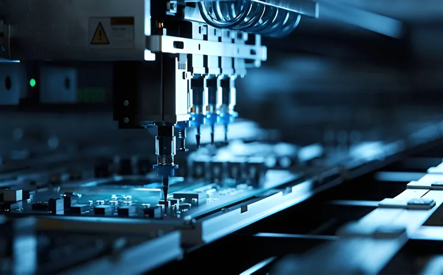
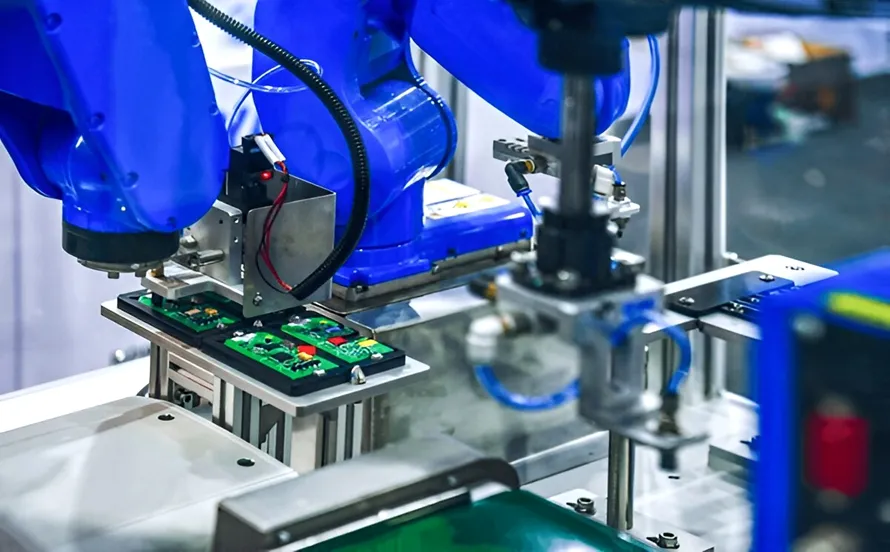
Automated pick-and-place equipment positions components according to the PCB assembly data.
Vision systems verify:
- Component identity
- Orientation
- Placement position
- Alignment
For high-reliability products, component placement accuracy is especially important for:
- Fine-pitch ICs
- BGA packages
- Power components
- High-density assemblies
3. Reflow Soldering
The assembled PCB is transferred through a controlled reflow oven.
A typical lead-free profile includes:
Preheat → Soak → Reflow → Cooling
The actual profile should be determined by:
- Solder paste specifications
- PCB materials
- Component thermal limits
- Board mass
- Copper distribution
- Assembly configuration
The goal is to achieve reliable solder wetting without causing:
- Component damage
- PCB warpage
- Delamination
- Excessive oxidation
- Poor solder-joint formation
4. THT Assembly
Through-hole components are inserted manually or automatically.
Depending on the design, soldering may use:
- Wave soldering
- Selective soldering
- Manual soldering
Selective soldering is particularly useful for mixed-technology assemblies because it limits thermal exposure to sensitive SMT components.
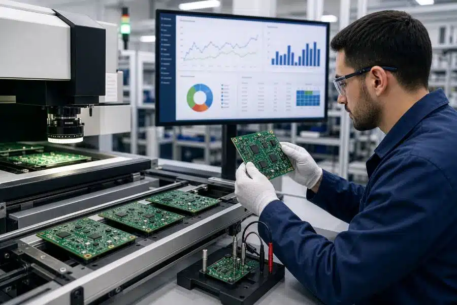
5. Inspection
Inspection is performed at several points throughout assembly.
AOI
Automated Optical Inspection (AOI) can identify:
- Missing components
- Incorrect placement
- Polarity errors
- Solder bridges
- Tombstoning
- Visible solder defects
X-Ray Inspection
For components with hidden solder joints, X-ray inspection is often required.
It can detect:
- BGA voids
- Insufficient solder
- Bridging
- Open solder joints
- Hidden alignment defects
6. Electrical Testing
Electrical testing verifies that the board has been assembled correctly.
Common methods include:
ICT
In-Circuit Testing (ICT) evaluates individual electrical nodes and component characteristics using a dedicated fixture.
Flying Probe Testing
Flying probe systems use movable probes and are particularly useful for prototypes and low-volume production because dedicated fixtures may not be necessary.
Functional Testing
FCT (Functional Circuit Testing) evaluates the completed PCBA under operating conditions.
It may verify:
- Power consumption
- Communication interfaces
- Sensor functions
- Displays
- Motors
- RF interfaces
- Digital signals
- Firmware operation
Best Practices for High-Reliability PCB Assembly
1. Maintain PCB and Manufacturing Cleanliness
Cleanliness is one of the most important factors in high-reliability electronics.
Contamination can contribute to:
- Corrosion
- Leakage current
- Electrochemical migration
- Poor solderability
- Insulation degradation
This becomes increasingly important as PCB geometries become smaller.
Manufacturers should control:
- Ionic contamination
- Flux residues
- Dust
- Moisture
- Foreign materials
- Handling contamination
Proper ESD control should also be implemented throughout production.
2. Select Materials Carefully
Material selection should be based on the actual application requirements.
For example:
- High-Tg FR-4 for elevated-temperature applications
- Low-loss laminates for high-speed/high-frequency designs
- Polyimide for flexible circuits
- Metal-core PCB for thermal management
- Heavy copper for high-current applications
Engineers should also consider:
- Tg
- CTE
- Moisture absorption
- Dielectric properties
- Thermal conductivity
- Flexibility
- Flame rating
3. Select the Right Solder Paste
Solder paste directly affects solder-joint reliability.
Important factors include:
- Alloy composition
- Powder particle size
- Flux chemistry
- Viscosity
- Shelf life
- Moisture sensitivity
- Reflow characteristics
For environmentally controlled products, lead-free alloys such as SAC systems are widely used.
Low-residue or halogen-free flux systems may also be selected when appropriate, although the correct chemistry depends on the application and required cleanliness level.
4. Control Component Storage and Handling
Electronic components can be damaged before they even enter the assembly line.
Manufacturers should control:
- Moisture sensitivity
- ESD protection
- Storage temperature
- Shelf life
- Date codes
- Packaging integrity
- Lot traceability
MSL (Moisture Sensitivity Level) management is particularly important for BGAs and other moisture-sensitive components.
Components with elevated MSL ratings may require controlled storage, baking, and floor-life management before reflow.
5. Optimize the Reflow Profile
High-reliability assembly should use a validated thermal profile rather than a generic oven setting.
Profile verification should consider:
- Peak temperature
- Ramp rate
- Soak duration
- Time above liquidus
- Cooling rate
Thermal profiling should be performed using representative production boards and thermocouple locations selected around temperature-sensitive components.
6. Use Design for Reliability
Design teams should address reliability before manufacturing begins.
Recommended practices include:
- Component derating
- Thermal simulation
- Adequate copper width
- Robust via design
- Appropriate spacing
- Stress relief around connectors
- Proper board support
- Controlled impedance where needed
- Avoiding unnecessary mechanical stress
DFM, DFA, and DFT reviews should be performed before prototype production.
7. Build and Qualify Prototypes
A production-intent prototype is one of the most effective methods for reducing manufacturing risk.
Prototype builds allow engineers to verify:
- Component selection
- Assembly process
- Reflow profile
- Thermal performance
- Functional performance
- Mechanical fit
- Test coverage
- Manufacturing yield
Design issues are significantly easier and less expensive to correct before high-volume production.
Reliability Testing for PCB Assembly
High-reliability electronics may require additional testing beyond standard production inspection.
Thermal Cycling
Boards are repeatedly exposed to temperature extremes to evaluate:
- Solder-joint durability
- Via reliability
- Lamination integrity
- CTE-related stress
Burn-In Testing
Boards operate under elevated temperature and electrical stress for a defined period.
Burn-in can help identify early-life failures before products reach customers.
Humidity Testing
Humidity exposure can reveal:
- Corrosion
- Insulation degradation
- Leakage
- Moisture-related reliability issues
Vibration and Mechanical Shock
Automotive, aerospace, industrial, and defense products may need mechanical testing to confirm that components and solder joints remain secure during vibration and shock.
Standards Relevant to High-Reliability PCB Assembly
Depending on the industry, customers may reference multiple standards.
Common examples include:
IPC-A-610 — Acceptability of Electronic Assemblies
IPC J-STD-001 — Requirements for Soldered Electrical and Electronic Assemblies
IPC-6012 — Qualification and Performance Specification for Rigid Printed Boards
IPC-2221 — Generic Standard on Printed Board Design
For specialized industries, additional quality-management and product-specific standards may apply, such as:
- ISO 9001
- ISO 13485
- IATF 16949
- AS9100
- ISO 26262
The correct compliance framework should be determined from the end product, market, and customer requirements rather than assuming one standard applies to every project.
Common High-Reliability PCB Assembly Defects
Solder Bridging
Excess solder can connect neighboring pads and create electrical shorts.
Common causes:
- Excessive solder-paste volume
- Incorrect stencil aperture design
- Poor component placement
- Improper reflow conditions
Solution: Optimize stencil design, solder-paste deposition, placement accuracy, and reflow profile.
Component Misalignment
Components may shift during placement or reflow.
Common causes:
- Poor paste balance
- Incorrect placement coordinates
- Uneven heating
- Poor pad geometry
Solution: Improve stencil design, machine calibration, placement accuracy, and thermal uniformity.
Poor Wetting
Poor solder wetting can produce weak electrical and mechanical joints.
Potential causes include:
- Oxidized surfaces
- Contaminated pads
- Incorrect flux chemistry
- Improper thermal profile
- Expired solder paste
Strict control of component storage, PCB cleanliness, solder paste condition, and reflow parameters can reduce this risk.
Tombstoning
Small passive components can stand on one end during reflow.
Typical causes include:
- Uneven solder volume
- Uneven pad geometry
- Thermal imbalance
- Incorrect placement
Optimized stencil apertures and thermal profiles help reduce the problem.
How to Choose a High-Reliability PCB Assembly Manufacturer
Choosing the right high-reliability PCB assembly manufacturer is critical because supplier capability directly affects product reliability.
Consider the following factors.
Engineering Capability
The supplier should provide:
- DFM/DFA review
- DFT analysis
- Stack-up review
- Thermal analysis
- BOM verification
- Component lifecycle analysis
- Manufacturing optimization
Advanced Manufacturing Equipment
A capable supplier should have access to:
- SPI
- High-precision SMT placement
- Controlled reflow ovens
- AOI
- X-ray
- ICT
- FCT
- Selective soldering
- Environmental testing where required
Traceability
For high-reliability products, production traceability should ideally connect:
Component Lot → Assembly Process → Machine → Operator → Inspection Result → Test Result → Finished Product
This makes root-cause analysis and field-service management significantly more effective.
Quality Management
Look for appropriate quality systems and certifications based on the target application.
For medical electronics, for example, ISO 13485 may be relevant. For automotive products, IATF 16949 may be required. Aerospace programs may require AS9100.
Why Choose Kingda for High-Reliability PCB Assembly?
Kingda provides one-stop PCB manufacturing and PCBA assembly services, covering PCB fabrication, component sourcing, SMT assembly, THT assembly, inspection, functional testing, and production support.
For reliability-sensitive applications, Kingda’s capabilities can help customers manage the entire manufacturing process rather than coordinating several separate suppliers.
Engineering and DFM Support
Kingda provides engineering support covering DFM, DFA, BOM review, component selection, manufacturing optimization, and production preparation.
This helps identify manufacturing risks before they become production problems.
Advanced Assembly and Inspection
Kingda’s published capabilities include:
- SMT assembly
- THT assembly
- Fine-pitch component assembly
- BGA/QFN assembly
- SPI
- AOI
- X-ray inspection
- ICT
- Functional testing
- Conformal coating
- IC programming
These capabilities support products requiring higher levels of assembly accuracy and inspection coverage.
Broad PCB Manufacturing Capability
Kingda supports different PCB technologies, including:
- Rigid PCB
- Multilayer PCB
- HDI PCB
- Flexible PCB
- Rigid-flex PCB
- Aluminum PCB
- High-frequency PCB
This allows engineers to select PCB structures based on electrical, thermal, mechanical, and environmental requirements.
Quality Certifications
Kingda states that it maintains certifications including ISO 9001, ISO 13485, IATF 16949, ISO 14001 and UL certification, supporting projects in medical, automotive, industrial, and other specialized applications.
Prototype-to-Production Support
A major advantage of working with an integrated manufacturer is the ability to maintain engineering and manufacturing continuity from prototype PCB assembly through low-volume production and mass production.
This can reduce repeated supplier qualification and help preserve process knowledge as production scales.
Conclusion
High-reliability PCB assembly is not simply a more careful version of standard PCB assembly. It is a complete manufacturing strategy built around reliability, process control, material selection, inspection, testing, and traceability.
The most important practices include:
For automotive, medical, aerospace, industrial, communications, and defense electronics, these controls can significantly reduce manufacturing risk and improve long-term product performance.
Choosing an experienced high-reliability PCB assembly manufacture early in the development process is equally important. A capable partner can contribute not only assembly capacity, but also DFM support, component sourcing, process engineering, testing, quality management, and production scalability.
Kingda’s one-stop PCB manufacturing and PCBA capabilities provide an integrated path from engineering prototype to volume production, helping customers develop reliable electronic products while controlling manufacturing complexity.