Modern lighting systems are becoming brighter, smaller, more efficient, and more intelligent. From automotive headlights and commercial lighting to medical equipment, industrial indicators, LED displays, and smart-home products, LED PCB assembly plays a critical role in converting electronic designs into reliable lighting products.
Unlike conventional PCB assembly, LED PCB assembly requires much more attention to thermal management. LEDs convert electrical energy into light, but a significant portion of the input power is also converted into heat. If that heat cannot be effectively transferred away from the LED junction, light output may decrease, color characteristics may shift, and component lifetime may be significantly reduced.
For this reason, successful LED electronics design begins with the PCB itself. Material selection, thermal paths, substrate construction, solder mask, copper thickness, component placement, soldering profiles, and inspection must all work together.
This guide explains what LED PCB assembly is, which materials are commonly used, how the assembly process works, the major thermal and manufacturing challenges, and how to select a reliable LED PCB assembly manufacturer.
What Is LED PCB Assembly?
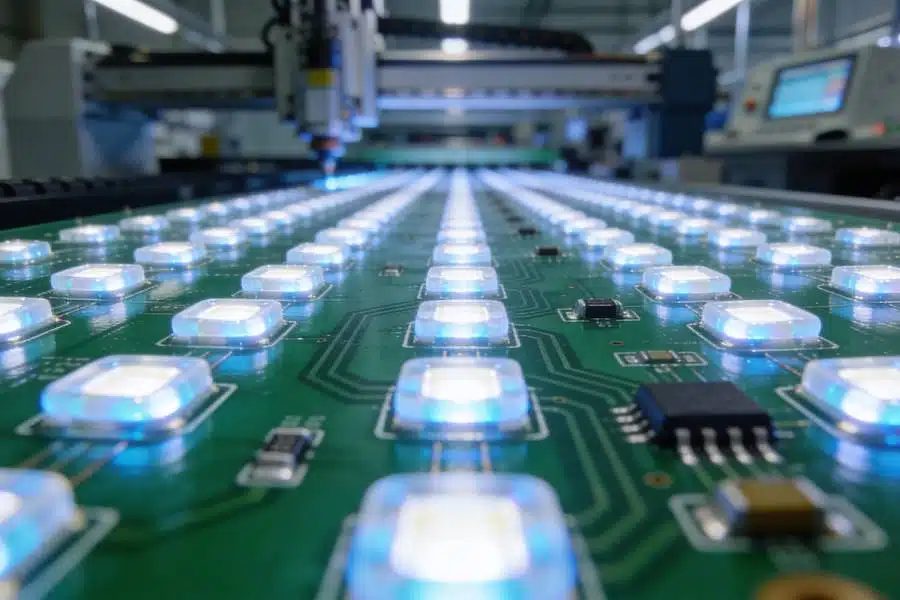
LED PCB assembly is the process of mounting and soldering LEDs, LED drivers, resistors, capacitors, controllers, connectors, and other electronic components onto a PCB specifically designed for lighting applications.
The major difference between ordinary PCB assembly and LED assembly is the importance of heat dissipation.
For a conventional low-power electronic board, thermal management may be focused primarily on processors, power ICs, or voltage regulators. In an LED application, the LED package itself is usually one of the key thermal sources.
Therefore, the PCB performs two functions simultaneously:
Electrical Function:
It distributes power and electrical signals between LEDs, drivers, controllers, and other components.
Thermal Function:
It provides a controlled path for transferring heat away from the LED package and into the surrounding structure or heat sink.
This is why an LED PCB should not be treated merely as a mounting platform.
Why Thermal Management Is Critical in LED PCB Assembly
LED lifetime and optical performance are strongly influenced by junction temperature. As operating temperature increases, LEDs can experience reduced luminous performance, color changes, accelerated material degradation, and shorter operating life.
A typical thermal path can be represented as:
LED Junction → LED Package → Solder Joint → PCB Copper → Dielectric → Metal Core → Heat Sink → Ambient Environment
Every layer in this path contributes thermal resistance.
A poorly designed PCB can create a thermal bottleneck even when the LED and driver have been selected correctly.
Important thermal-design factors include:
- PCB substrate material
- Thermal conductivity of the dielectric
- Copper thickness
- Thermal pad design
- Thermal vias
- Metal-core construction
- Heat-sink interface
- Component spacing
- Operating environment
- Airflow
For high-power lighting, thermal design should therefore be completed before final component placement and assembly.
LED PCB Materials
Material selection is one of the most important decisions in LED PCB manufacturing and assembly.
Aluminum Metal Core PCB
Aluminum PCB, also known as an MCPCB (Metal Core PCB), is one of the most common solutions for LED lighting.
An aluminum PCB typically contains:
Copper Circuit Layer → Dielectric Layer → Aluminum Base
The aluminum base provides a relatively efficient path for heat transfer compared with a conventional FR-4 construction.
Typical applications include:
- LED streetlights
- Automotive lighting
- High-power floodlights
- Commercial lighting
- High-bay lighting
- Outdoor lighting
- LED signage
For applications where heat generation is relatively high, aluminum MCPCB is generally more appropriate than standard FR-4.
Copper Core PCB
Copper-core PCBs provide even higher thermal conductivity than aluminum-core constructions and can be used in applications with demanding thermal loads.
They are suitable for:
- High-power LED arrays
- Automotive lighting
- High-current lighting systems
- High-density thermal designs
- Specialized industrial applications
However, copper-core PCBs are typically more expensive and can introduce additional manufacturing and weight considerations.
FR-4 LED PCB
FR-4 remains useful for low-power LED applications where thermal requirements are moderate.
Typical applications include:
- Indicator LEDs
- Small control boards
- Low-power lighting
- Consumer electronics
- Decorative electronics
FR-4 should not automatically be considered unsuitable for LED applications. The correct material depends on the electrical power, thermal load, operating environment, and mechanical structure of the final product.
Flexible LED PCB
Flexible LED circuits generally use polyimide or other flexible substrates.
They are useful for:
- Flexible LED strips
- Wearable lighting
- Curved lighting
- Automotive interior lighting
- Decorative lighting
- Compact medical devices
The main advantage is the ability to follow curved or irregular surfaces while maintaining electrical connectivity.
White Solder Mask and Optical Performance
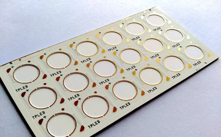
One important feature that differentiates many LED boards from conventional PCBs is white solder mask.
Because LED packages emit light in multiple directions, part of the light can interact with the PCB surface.
A reflective white solder mask can help redirect stray or side-emitted light toward the desired optical direction. This can contribute to improved optical efficiency depending on the LED package, optical design, surface properties, and lighting architecture.
For high-performance LED applications, engineers should therefore evaluate:
- Reflectivity
- Color stability
- Temperature resistance
- UV resistance
- Reflow compatibility
- Long-term aging characteristics
The solder mask is not simply a cosmetic choice. For some LED products, it is part of the optical and thermal design.
LED PCB Assembly Process
A reliable LED PCB assembly process generally follows several controlled stages.
1. Engineering Review and DFM
Before production begins, the manufacturer reviews:
- Gerber files
- BOM
- Pick-and-Place files
- Assembly drawings
- PCB stackup
- Thermal requirements
- Component specifications
The DFM/DFA review should identify potential issues involving:
- LED footprint
- Thermal pad geometry
- Component spacing
- Solder-mask openings
- PCB edge clearance
- Thermal vias
- Assembly orientation
- Component availability
For LED boards, thermal design should be included in the engineering review rather than treated as a later assembly problem.
2. Substrate Preparation
The PCB substrate is prepared according to the specified material.
For an aluminum MCPCB, this may involve controlled processing of:
- Aluminum base
- Dielectric layer
- Copper circuit layer
- Thermal interface structure
Surface cleanliness and dimensional stability are important because contamination or poor bonding can increase thermal resistance.
3. Stencil Preparation
A stainless-steel SMT stencil is manufactured according to the PCB pad geometry.
Stencil aperture design is particularly important for:
- LED thermal pads
- Large-area power pads
- Fine-pitch drivers
- Small passive components
Incorrect solder volume can cause voiding, poor solder joints, component movement, or thermal performance problems.
4. Solder Paste Printing
The stencil is aligned with the PCB and solder paste is deposited onto the required pads.
Important parameters include:
- Solder paste type
- Stencil thickness
- Aperture ratio
- Squeegee pressure
- Printing speed
- Board support
- Alignment accuracy
SPI (Solder Paste Inspection) can then verify the volume and location of solder paste deposits before placement.
5. Component Placement
Automated pick-and-place equipment mounts:
- LED packages
- LED drivers
- Resistors
- Capacitors
- Controllers
- Connectors
- Protection components
Placement accuracy is particularly important for LED arrays.
A small positional deviation may affect:
- Light distribution
- Optical alignment
- LED spacing
- Uniformity
- Thermal interface positioning
6. Reflow Soldering
The populated LED PCB enters a temperature-controlled reflow oven.
The thermal profile normally includes:
Preheat → Soak → Reflow → Cooling
Unlike ordinary SMT assembly, the thermal process for LED PCBs deserves additional attention because LED packages, phosphor materials, lenses, adhesives, and thermal interfaces may have specific temperature limitations.
The production team should optimize:
- Ramp rate
- Soak time
- Peak temperature
- Time above liquidus
- Cooling rate
The exact profile should always be based on the solder paste specification and component manufacturer’s thermal requirements rather than using one universal temperature curve.
7. AOI Inspection
After reflow, AOI (Automated Optical Inspection) checks the assembly.
Typical defects include:
- Missing LEDs
- Incorrect component orientation
- Misaligned components
- Solder bridges
- Tombstoning
- Insufficient solder
- Visible solder defects
8. X-Ray Inspection
For LED assemblies containing BGA, QFN or other hidden solder connections, X-ray inspection can provide additional internal inspection.
X-ray inspection may identify:
- Voids
- Hidden bridges
- Incomplete solder joints
- Insufficient solder
- Misalignment
9. Electrical and Functional Testing
The final LED assembly should be tested according to the application’s requirements.
Typical tests include:
- Input voltage
- Operating current
- LED brightness
- Color temperature
- LED uniformity
- Driver operation
- Dimming function
- Communication interfaces
- Thermal behavior
- Protection functions
For intelligent lighting systems, functional testing may also verify PWM dimming, communication protocols, sensors, wireless connectivity, and controller operation.
Common LED PCB Assembly Challenges
1. Insufficient Heat Dissipation
This is one of the most serious problems.
If thermal resistance is too high, the LED junction temperature can rise excessively.
Potential consequences include:
- Reduced brightness
- Color shift
- Shorter lifetime
- Driver instability
- PCB degradation
- Thermal runaway in certain systems
The solution is to optimize the entire thermal path rather than simply adding a larger heat sink.
2. Poor Thermal Interface
Even when an aluminum PCB is selected, poor bonding between the copper circuit, dielectric, and metal core can reduce thermal performance.
Voids and inconsistent dielectric thickness can become thermal barriers.
3. Solder Voiding
Large thermal pads beneath LED packages can be prone to solder voids.
Excessive voiding can increase thermal resistance between the component and PCB.
Engineers can address this through:
- Optimized stencil apertures
- Windowpane patterns
- Controlled solder volume
- Reflow optimization
- X-ray inspection
4. LED Misalignment
In high-density LED arrays, incorrect placement can cause inconsistent illumination.
High-precision placement and appropriate fiducial design are therefore important.
5. Solder Mask Aging
In high-temperature or UV-exposed applications, poorly selected solder-mask materials can lose reflectivity or experience discoloration.
For long-life lighting products, engineers should evaluate material stability throughout the expected operating temperature and lifetime.
LED PCB Applications
LED PCB assembly is widely used in many industries.
Automotive Lighting
Applications include:
- Headlights
- Taillights
- Daytime running lights
- Interior lighting
- Dashboard illumination
Automotive lighting requires strong thermal performance, vibration resistance, reliability, and controlled manufacturing processes.
Commercial and Residential Lighting
LED PCBs are used in:
- Downlights
- Panel lights
- Streetlights
- Floodlights
- Linear lighting
- High-bay lighting
LED Displays and Signage
Large LED displays and signage systems require large numbers of LED components and consistent thermal and electrical performance.
Medical Equipment
LED lighting is used in diagnostic and medical equipment where optical consistency and reliability are important.
Industrial Equipment
LED boards are used for:
- Machine indicators
- Industrial lighting
- Control panels
- Inspection equipment
- High-temperature environments
How to Choose an LED PCB Assembly Manufacturer
Choosing an experienced LED PCB assembly manufacturer early in the project can prevent expensive redesigns later.
1. Verify Thermal Manufacturing Capabilities
Ask the manufacturer whether it can support:
- Aluminum MCPCB
- Copper-core PCB
- High-Tg materials
- Thermal vias
- Thermally optimized PCB structures
- Customized stackups
Kingda’s PCB manufacturing capabilities include aluminum PCB, copper-base PCB, FR-4, high-frequency PCB, flexible PCB, rigid-flex PCB and HDI PCB, giving engineers multiple substrate options for different applications. (Kingda)
2. Evaluate SMT Assembly Equipment
A capable LED PCB assembly supplier should have:
- High-speed pick-and-place machines
- 3D SPI
- AOI
- X-ray
- Controlled reflow ovens
- Precision stencil technology
Kingda reports 8 fully automatic SMT production lines, 3D SPI, AOI and X-ray inspection equipment, as well as a twelve-zone reflow oven for SMT quality control. (Kingda)
3. Look for Engineering Support
The manufacturer should be able to review:
- Gerber files
- BOM
- PCB stackup
- Component availability
- Thermal design
- Assembly design
- Testing requirements
Kingda provides DFM-oriented engineering support and component sourcing as part of its integrated manufacturing model. (Kingda)
4. Check Quality and Traceability
For professional LED products, quality management should include multiple inspection stages.
Kingda’s published quality system includes SPI, AOI, X-ray, FAI, ICT and FCT, together with manufacturing traceability from incoming materials through final shipment. (Kingda)
5. Consider Production Scalability
A suitable partner should support the complete product lifecycle:
Prototype → Low Volume → Pilot Production → Mass Production
Kingda states that it supports prototype, low-volume, and volume PCB assembly, allowing projects to transition from development into production without necessarily changing manufacturing partners. (Kingda)
Why Choose Kingda for LED PCB Assembly?
Kingda is a one-stop PCB and PCBA manufacturer founded in 2013, integrating PCB fabrication, component procurement, SMT, DIP, product assembly and testing under one manufacturing model. (Kingda)
For LED and other specialized electronics projects, key advantages include:
One-Stop Manufacturing
Kingda can integrate PCB manufacturing, component sourcing and assembly, reducing communication between multiple suppliers and simplifying project management. (Kingda)
Aluminum and Metal-Core PCB Capability
Kingda’s PCB manufacturing portfolio includes aluminum PCB and copper-base PCB, providing material options for LED and other thermally demanding applications. (Kingda)
Advanced SMT Assembly
Kingda reports support for fine-pitch packages and miniature components, along with 8 automated SMT lines and advanced inspection equipment. (Kingda)
Comprehensive Testing
Kingda’s published inspection capabilities include 3D SPI, AOI, X-ray, FAI, ICT and FCT, allowing inspection strategies to be matched to product complexity and reliability requirements. (Kingda)
Industry Certifications
Kingda states that it holds ISO 9001, ISO 13485, IATF 16949, ISO 14001 and UL certification, with IPC-A-610 and environmental compliance requirements incorporated into its quality system. (Kingda)
Prototype to Mass Production
Kingda supports rapid PCBA prototyping and production programs. Its published prototype capabilities include 01005/0201 components, 0.25 mm-pitch BGA, SMT/THT/mixed assembly, AOI, X-ray, ICT and FCT. (Kingda)
LED PCB Assembly Cost Factors
The cost of an LED PCB assembly project depends on more than PCB size.
| Cost Factor | Impact on Cost |
|---|---|
| PCB substrate | Aluminum and copper-core PCBs generally cost more than basic FR-4 |
| PCB thickness | Thicker copper or dielectric structures can increase cost |
| LED package | Fine-pitch and high-power LED packages require more precise processes |
| Solder mask | Specialized white or high-reflectivity solder masks can add material cost |
| Stencil | Complex apertures and fine-pitch designs may require specialized stencil manufacturing |
| Assembly volume | Larger production quantities generally reduce the unit assembly cost |
| Inspection | X-ray, ICT, FCT and specialized testing add cost but improve quality assurance |
| Component sourcing | Obsolete or long-lead components can increase procurement costs |
| Thermal requirements | Advanced MCPCB structures and thermal solutions can increase manufacturing complexity |
The cheapest PCB is not necessarily the lowest-cost solution. A board with poor thermal performance can create much higher costs through field failures, warranty claims, redesigns and replacement programs.
LED PCB Assembly: Best Practices
For a successful LED PCB project, consider these principles from the beginning:
1. Design the thermal path before routing the electrical circuit.
2. Select the PCB substrate according to actual power and thermal requirements.
3. Use aluminum or copper-core construction when thermal loading demands it.
4. Optimize thermal-pad and stencil aperture design to reduce solder voiding.
5. Select a stable white solder mask when optical reflectivity is important.
6. Validate the complete reflow profile with the actual LED and solder-paste combination.
7. Use AOI and X-ray where the package and application justify them.
8. Perform functional testing under realistic electrical and thermal conditions.
9. Involve the PCB assembly manufacturer during the design stage rather than after the PCB is finished.
Conclusion
LED PCB assembly is fundamentally different from conventional PCB assembly because thermal management and optical performance must be considered alongside electrical and mechanical requirements.
The most successful designs treat the PCB as part of the lighting system rather than simply a platform for mounting LEDs.
From MCPCB materials and thermal interfaces to white solder mask, stencil design, component placement, reflow soldering, AOI, X-ray and functional testing, each manufacturing stage contributes to the final performance and lifetime of the LED product.
For companies developing LED lighting, automotive lighting, industrial equipment, medical electronics or intelligent lighting systems, selecting an experienced LED PCB assembly manufacturer early can significantly reduce engineering risks and manufacturing rework.
With PCB fabrication, component sourcing, advanced SMT/THT assembly, inspection, testing and production capabilities integrated under one system, Kingda provides a one-stop manufacturing platform capable of supporting electronics projects from prototype through volume production. (Kingda)