The rapid development of artificial intelligence (AI), 5G communications, high-performance computing, cloud infrastructure, autonomous vehicles, and the Internet of Things (IoT) is pushing electronic systems toward higher data rates, greater processing power, and increasingly compact designs.
At the center of this evolution is the high-speed PCB. Modern high-speed circuit boards must transmit large volumes of data while maintaining signal quality, timing accuracy, power stability, and electromagnetic compatibility.
Unlike conventional PCB designs, high-speed PCB design requires engineers to consider transmission-line effects, controlled impedance, signal integrity, return paths, crosstalk, power integrity, thermal management, and manufacturing tolerances from the earliest design stage.
This guide explains what a high-speed PCB is, the most important high-speed PCB design principles, manufacturing and assembly requirements, common challenges, applications, testing methods, and the advantages of choosing an experienced manufacturing partner such as Kingda.
What Is a High-Speed PCB?
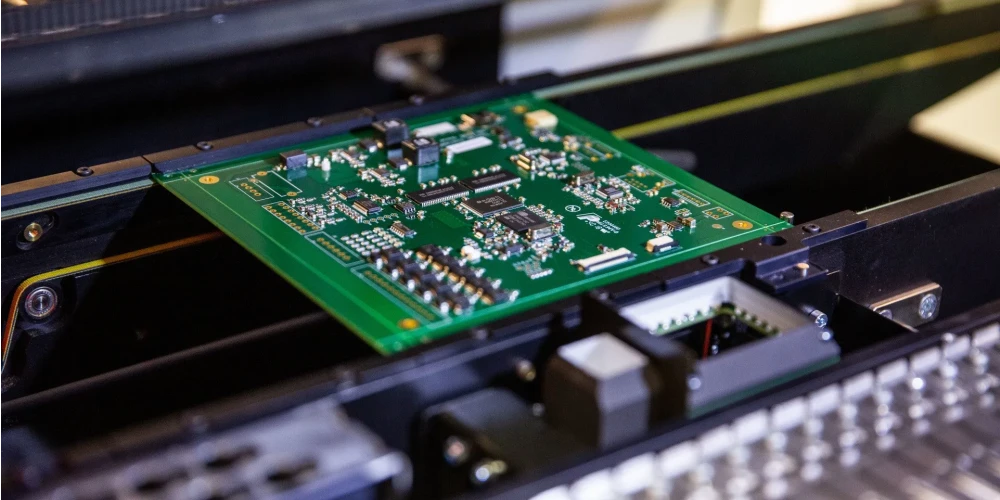
A high-speed PCB is a printed circuit board designed to transmit and process high-speed electrical signals where signal-integrity effects can significantly influence system performance.
A common misconception is that a PCB becomes “high speed” only when it exceeds a particular frequency. In practice, signal rise time, fall time, edge rate, trace length, and interconnect geometry are equally important.
As signal edges become faster, PCB traces increasingly behave as transmission lines rather than simple wires. This makes the following parameters critical:
- Controlled impedance
- Signal integrity
- Power integrity
- Propagation delay
- Crosstalk
- Reflection
- Return-path continuity
- EMI/EMC performance
Typical applications of high-speed PCBs include:
- AI servers and accelerators
- Data-center networking equipment
- High-performance computing systems
- 5G communication equipment
- Network switches and routers
- Storage systems
- Automotive electronics
- ADAS and autonomous-driving systems
- Medical imaging equipment
- Industrial control systems
- Consumer electronics
High-speed interfaces may include DDR, PCIe, USB, Ethernet, SerDes, MIPI, HDMI, DisplayPort, LVDS, and other high-data-rate protocols.
Why High-Speed PCB Design Is More Challenging
At relatively low speeds, a PCB trace can often be treated as an ordinary conductive path. As edge rates increase, however, the electrical characteristics of the interconnect become more important.
Impedance discontinuities at vias, connectors, layer transitions, trace-width changes, and component packages can produce reflections and waveform distortion.
A successful high-speed PCB design therefore needs to coordinate several engineering disciplines:
Signal Integrity + Power Integrity + Impedance Control + Return Path + Thermal Management + EMI/EMC + Manufacturing
These parameters are interconnected.
For example, changing dielectric thickness changes characteristic impedance, which affects the PCB stackup and potentially the overall board thickness. Changing a trace route may improve signal integrity but introduce a poor return path or create additional crosstalk.
Key High-Speed PCB Design Principles
1. Signal Integrity
Signal integrity (SI) is one of the most important considerations in high-speed PCB design.
The objective is to deliver signals to the receiver with acceptable:
- Voltage levels
- Timing margins
- Rise and fall times
- Noise margins
- Jitter
- Waveform shape
Potential problems include:
- Reflections
- Overshoot
- Undershoot
- Ringing
- Crosstalk
- Insertion loss
- Excessive attenuation
For critical interfaces, engineers should analyze the complete channel from transmitter to receiver rather than considering only the PCB trace.
2. Controlled Impedance
Controlled impedance PCB design keeps the characteristic impedance of high-speed traces within the required range.
Common target values include:
- 50 Ω single-ended
- 85 Ω differential
- 90 Ω differential
- 100 Ω differential
The correct target must always be based on the interface specification and system architecture.
Characteristic impedance is affected by:
- Trace width
- Copper thickness
- Dielectric thickness
- Dielectric constant
- Copper roughness
- Reference-plane distance
- Stackup construction
Therefore, impedance should be designed together with the PCB manufacturer rather than treated purely as an EDA calculation.
Kingda supports high-speed and high-frequency PCB manufacturing, including multilayer structures, controlled manufacturing parameters, HDI structures, and high-speed communication applications. (GoPCBA)
3. Return Path Management
Every high-speed signal requires an appropriate return-current path.
A typical high-speed structure is:
High-Speed Signal Layer → Continuous Ground/Reference Plane
Problems may occur when a signal crosses:
- Plane splits
- Large voids
- Reference-plane gaps
- Poorly designed anti-pads
- Unnecessary layer transitions
A disrupted return path increases loop area and can increase EMI, crosstalk, and signal-integrity problems.
For this reason, maintaining a continuous reference plane is one of the most important principles in high-speed PCB routing.
4. Differential Pair Routing
Many modern high-speed interfaces use differential signaling.
A differential pair uses two traces carrying complementary signals. Maintaining consistent geometry between these traces helps preserve common-mode noise rejection and signal timing.
Important parameters include:
- Pair spacing
- Trace width
- Differential impedance
- Intra-pair length matching
- Skew
- Layer transitions
- Via symmetry
- Reference-plane continuity
Differential routing is commonly used for interfaces such as:
- PCIe
- USB
- Ethernet
- HDMI
- DisplayPort
- LVDS
- High-speed SerDes
The objective is to maintain consistent electrical geometry from transmitter to receiver.
5. Crosstalk Control
Crosstalk occurs when energy from one signal couples into a neighboring signal.
It becomes more problematic when traces are:
- Closely spaced
- Long and parallel
- Carrying fast signal edges
- Routed over inappropriate reference structures
Methods for reducing crosstalk include:
- Increasing trace spacing
- Minimizing parallel routing
- Using appropriate ground/reference planes
- Separating sensitive and noisy signals
- Reducing unnecessary layer transitions
- Optimizing stackup geometry
Rather than relying on one universal spacing rule, engineers should validate critical designs with signal-integrity simulation.
High-Speed PCB Stackup Design
The PCB stackup is the foundation of electrical performance.
A properly engineered high-speed PCB stackup defines the relationship between:
- Signal layers
- Ground planes
- Power planes
- Dielectric materials
- Copper thickness
Important considerations include:
Signal-to-Plane Spacing
Keeping high-speed signal layers close to a reference plane helps control impedance and reduce electromagnetic coupling.
Dielectric Thickness
Dielectric thickness strongly affects impedance. Consistent manufacturing thickness is therefore important for repeatable high-speed performance.
Power Distribution
Modern CPUs, GPUs, FPGAs, memories, and communication processors may contain multiple power domains. The PCB must provide a stable power-distribution network.
Copper Thickness
Copper thickness influences resistance, current capacity, thermal performance, and impedance.
Kingda’s published PCB capability includes standard multilayer fabrication up to 20 layers and advanced constructions up to 100 layers, with fine-line structures, laser drilling, stacked microvias, and copper-filled microvias available in its stated advanced ranges. (GoPCBA)
Material Selection for High-Speed PCBs
Material selection directly influences signal loss, impedance stability, thermal performance, and reliability.
Standard FR-4
FR-4 remains suitable for many digital PCB designs.
However, more demanding systems may require specialty materials with better:
- Dielectric stability
- Lower dissipation factor
- Lower signal loss
- Thermal stability
- Dimensional stability
High-Frequency and Low-Loss Materials
For RF, microwave, networking, and demanding high-speed digital applications, low-loss laminates may be selected.
Important material parameters include:
- Dielectric constant (Dk)
- Dissipation factor (Df)
- Copper roughness
- Moisture absorption
- Thermal expansion
- Temperature stability
Material selection should be based on actual channel-performance requirements rather than simply choosing the most expensive material.
High-Speed PCB Manufacturing Process
The manufacturing process must reproduce the physical parameters used during electrical design.
A typical workflow includes:
Design Review → Stackup Engineering → Inner-Layer Imaging → Lamination → Drilling → Copper Plating → Outer-Layer Imaging → Etching → Solder Mask → Surface Finish → Electrical Testing → Final Inspection
1. Stackup Development
The fabricator determines:
- Layer count
- Dielectric thickness
- Copper weight
- Material type
- Impedance targets
- Lamination structure
For controlled-impedance boards, the fabricator should verify target impedance using actual production parameters.
2. Precision Drilling
Vias introduce discontinuities into high-speed signal paths.
Important parameters include:
- Drill diameter
- Pad size
- Annular ring
- Via type
- Via stub length
- Registration accuracy
Depending on the application, engineers may use:
- Blind vias
- Buried vias
- Microvias
- Back-drilled vias
3. Copper Plating
Copper plating forms conductive paths through plated holes and vias.
Consistent plating thickness is important for:
- Electrical conductivity
- Via reliability
- Current capacity
- Long-term durability
4. Outer-Layer Imaging and Etching
The outer circuitry is formed through imaging, plating, and etching processes.
Trace-width accuracy is particularly important for high-speed controlled-impedance structures.
5. Solder Mask and Surface Finish
Solder mask protects exposed copper and helps prevent solder bridges during assembly.
Surface finishes may include:
- ENIG
- HASL
- OSP
- Immersion Silver
- ENEPIG
The appropriate finish depends on solderability, component pitch, reliability requirements, environmental conditions, and cost.
High-Speed PCB Assembly
PCB fabrication is only one part of producing a reliable high-speed electronic system.
A typical high-speed PCB assembly workflow includes:
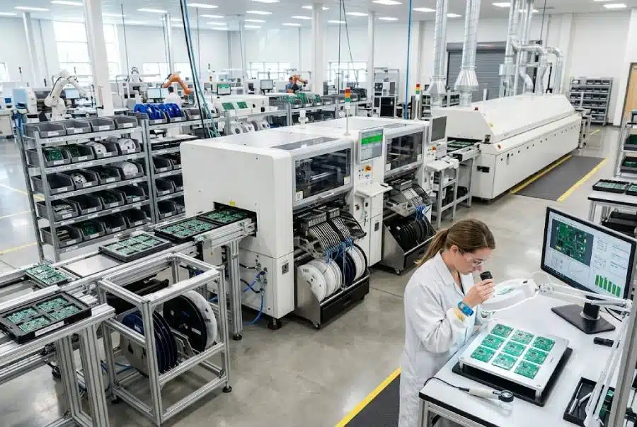
Solder Paste Printing → SPI → Component Placement → Reflow → AOI → X-Ray → ICT/FCT
Component Placement
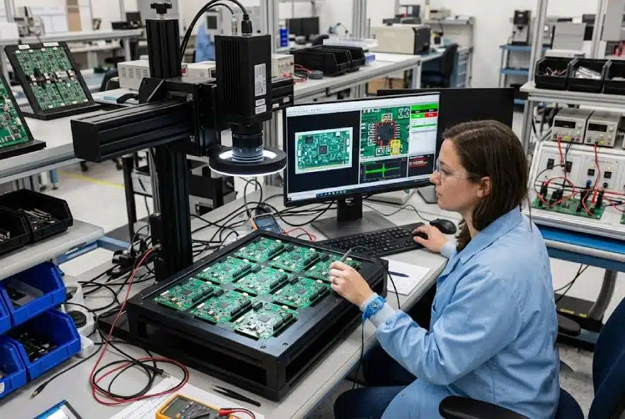
Component placement should follow signal-flow requirements.
High-speed processors, memory devices, transceivers, connectors, and clocking components should be positioned to minimize:
- Signal-path length
- Layer transitions
- Unnecessary vias
- Crosstalk
- Return-path discontinuities
Kingda supports advanced SMT assembly, including 01005 components, fine-pitch packages, BGA, QFN, CSP, LGA, PoP, and double-sided assembly. (GoPCBA)
Reflow Soldering
A validated thermal profile is essential.
Important parameters include:
- Ramp rate
- Preheat
- Soak
- Peak temperature
- Time above liquidus
- Cooling rate
Poor reflow control can produce solder defects that directly affect the electrical performance of high-density assemblies.
AOI and X-Ray Inspection
AOI can detect:
- Missing components
- Incorrect orientation
- Misalignment
- Solder bridges
- Visible solder defects
X-ray inspection provides internal visibility for hidden solder joints in BGA, QFN, CSP, and similar packages.
Kingda’s published inspection capabilities include SPI, AOI, X-ray, FAI, ICT, and FCT. (GoPCBA)
Simulation and Analysis
Simulation allows engineers to identify problems before fabricating expensive prototypes.
Signal Integrity Simulation
SI analysis can evaluate:
- Eye diagrams
- Reflections
- Crosstalk
- Insertion loss
- Return loss
- Propagation delay
- Jitter
- Timing margin
Power Integrity Simulation
Power integrity (PI) analysis evaluates:
- PDN impedance
- Voltage ripple
- Decoupling effectiveness
- Resonance
- Transient response
Thermal Analysis
High-performance processors, FPGAs, GPUs, memory devices, and power regulators can generate significant heat.
Thermal analysis helps engineers evaluate:
- Hot spots
- Copper heat spreading
- Thermal-via placement
- Heat sinks
- Airflow
- Component temperature
Applications of High-Speed PCBs
AI and Data Centers
AI accelerators and server infrastructure require high-bandwidth communication between processors, memory, networking devices, and storage.
5G Communications
5G infrastructure uses high-speed digital and RF circuits to process large volumes of data.
High-Performance Computing
HPC systems require high-speed interconnects between processors, memory, storage, and networking components.
Automotive Electronics
Modern vehicles increasingly depend on high-speed communication between:
- Cameras
- Radar
- Domain controllers
- ADAS systems
- Infotainment
- Vehicle networks
Medical Electronics
Medical imaging systems and advanced diagnostic devices require accurate and reliable transmission of large amounts of sensor and image data.
Industrial Automation
Industrial controllers, machine-vision systems, robotics, and industrial networking increasingly require high-speed data interfaces.
High-Speed PCB vs. Standard PCB
| Feature | High-Speed PCB | Standard PCB |
|---|---|---|
| Primary objective | High-speed signal transmission | General electrical connectivity |
| Impedance control | Usually critical | Often less demanding |
| Stackup | Carefully engineered | Generally simpler |
| Return path | Critical | Less demanding |
| Crosstalk | Must be controlled | Usually less significant |
| Material | May require low-loss laminates | FR-4 commonly sufficient |
| SI/PI simulation | Frequently recommended | Often limited |
| Manufacturing tolerance | Tighter | Generally less demanding |
| Cost | Higher | Lower |
| Applications | AI, 5G, HPC, networking, automotive | General electronics |
Common High-Speed PCB Problems and Solutions
Signal Reflection
Cause: Impedance discontinuities.
Potential solutions:
- Optimize trace geometry
- Match impedance
- Reduce abrupt width changes
- Improve via transitions
- Optimize termination
Via Stubs
Long via stubs may create unwanted resonant behavior.
Solutions: Use blind vias, buried vias, microvias, or back-drilling where appropriate.
Crosstalk
Cause: Excessively close or parallel high-speed routing.
Solutions: Increase spacing, reduce parallel routing, optimize reference planes, and perform SI simulation.
Return-Path Discontinuity
Cause: Signal crossing plane splits or gaps.
Solution: Maintain a continuous reference plane and provide appropriate return-current paths.
Power Integrity Problems
Cause: Poor power-distribution or inadequate decoupling.
Solutions:
- Improve PDN design
- Optimize capacitor placement
- Reduce power-loop inductance
- Analyze PDN impedance
- Improve power/ground-plane structure
High-Speed PCB Design Best Practices
A practical workflow for high-speed PCB design is:
Requirements → Stackup → Component Placement → Critical Routing → SI/PI Simulation → DRC → DFM → Prototype → Testing → Optimization
Recommended practices include:
- Define impedance targets before routing.
- Develop the PCB stackup with the fabricator.
- Place processors, memories, connectors, and transceivers according to signal flow.
- Keep high-speed traces short and direct.
- Minimize unnecessary vias.
- Maintain continuous reference planes.
- Match differential-pair lengths where required.
- Keep sensitive signals away from noisy circuits.
- Simulate critical channels.
- Perform DFM before manufacturing.
Quality Control for High-Speed PCB Manufacturing
A qualified high-speed PCB manufacturer should combine process control with electrical verification.
Fabrication Inspection
- AOI
- Dimensional inspection
- Copper-thickness verification
- Plating inspection
- Cross-section analysis
- Surface-finish inspection
Electrical Testing
- Continuity testing
- Isolation testing
- Flying-probe testing
- Fixture-based testing
- Controlled-impedance testing
PCBA Inspection
- SPI
- AOI
- X-ray
- ICT
- FCT
The actual test plan should be determined by the application’s performance and reliability requirements.
Why Choose Kingda for High-Speed PCB?
Kingda provides a one-stop PCB manufacturing and PCBA solution, integrating PCB design, fabrication, component procurement, SMT/THT assembly, inspection, testing, and final product integration. This reduces the need to coordinate separate suppliers and helps maintain engineering continuity from prototype to production. (GoPCBA)
Advanced High-Speed and High-Frequency PCB Capability
Kingda’s published PCB manufacturing capabilities include HDI PCB, high-frequency PCB, high-speed PCB, flexible PCB, rigid PCB, rigid-flex PCB, and multilayer PCB solutions. (GoPCBA)
Its published capabilities include fine-line structures, laser drilling, stacked microvias, copper-filled microvias, and advanced multilayer constructions. (GoPCBA)
Advanced SMT Assembly
Kingda supports:
- 01005 components
- 0201 components
- BGA
- Fine-pitch packages
- QFN
- CSP
- LGA
- PoP
- Double-sided SMT
Kingda also provides prototype, low-volume, and mass-production assembly services. (GoPCBA)
Engineering and DFMA Support
Kingda provides DFM and DFA, BOM verification, Gerber review, Pick-and-Place verification, component availability analysis, alternative-component recommendations, and manufacturing optimization. (GoPCBA)
This early engineering involvement can help identify manufacturability risks before they cause production delays.
Comprehensive Inspection and Testing
Kingda’s published quality system includes:
IQC → SPI → SMT/THT Assembly → AOI → X-Ray → ICT/FCT → OQC
Inspection capabilities include 3D SPI, AOI, X-ray, FAI, ICT, and FCT. (GoPCBA)
Quality Certifications
Kingda states that it maintains ISO 9001, ISO 13485, IATF 16949, ISO 14001, and UL certification, and is an IPC member. (GoPCBA)
These quality systems support applications including automotive, medical, industrial automation, AI, telecommunications, power electronics, and other reliability-sensitive products. (GoPCBA)
Prototype-to-Mass-Production Support
Kingda supports the complete manufacturing lifecycle from rapid PCBA prototyping and low-volume production to high-volume manufacturing, providing customers with a single manufacturing partner as their products scale. (GoPCBA)
Conclusion
The development of AI, 5G, high-performance computing, autonomous vehicles, advanced networking, and other data-intensive technologies is making high-speed PCB technology increasingly important.
A successful high-speed PCB is not simply a multilayer board with fast components. It requires coordinated engineering across:
Signal Integrity + Power Integrity + Controlled Impedance + Return Paths + Stackup + Materials + Thermal Management + Manufacturing + Assembly + Testing
Designing these factors together from the beginning can significantly reduce signal-integrity problems, manufacturing risks, redesigns, and time-to-market.
Working with an experienced manufacturer early in the design process is equally important. Kingda combines high-speed and high-frequency PCB manufacturing, HDI capability, advanced SMT/THT assembly, component sourcing, engineering support, inspection, and testing in a one-stop manufacturing model, supporting the transition from prototype PCB to production-ready high-speed PCBA. (GoPCBA)