What Is an IC Substrate PCB?
An IC substrate PCB is a high-density interconnection structure used between an integrated circuit (IC) and the next level of electronic interconnection, such as a printed circuit board or electronic package. Unlike a conventional PCB, an IC substrate is designed for extremely fine-pitch connections, high wiring density, electrical performance, thermal management, and reliable semiconductor packaging.
IC substrates are widely used with advanced package technologies such as PBGA, FCBGA, FC-CSP, and WBCSP. They provide the electrical and mechanical interface between the semiconductor die or package and the main circuit board.
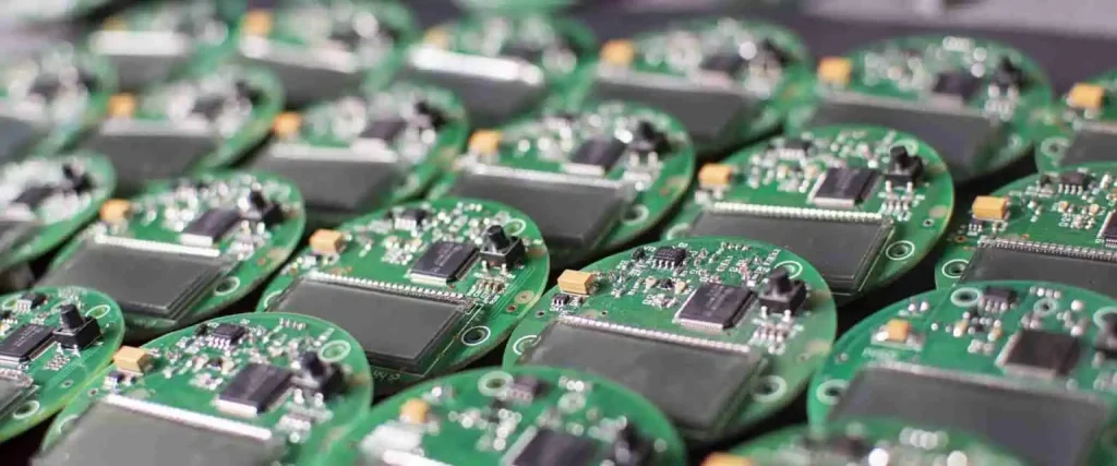
As semiconductor devices continue to increase in transistor density while package dimensions become smaller, conventional PCB technologies may not provide sufficient routing density. An IC substrate PCB manufacturer therefore needs advanced fabrication technologies, precise registration control, fine-line imaging, microvia processing, sequential lamination, and stringent inspection systems.
For projects that require different high-density circuit structures, manufacturers may also combine IC substrate technologies with HDI PCB manufacturing, depending on the electrical and mechanical requirements of the final product.
Why Are IC Substrates Important in Semiconductor Packaging?
An IC substrate acts as an intermediate interconnection platform between the semiconductor package and the system-level PCB.
The substrate performs several important functions:
- Provides electrical connections between the IC and PCB
- Distributes power and ground connections
- Supports high-density signal routing
- Helps manage signal integrity
- Provides mechanical support for the package
- Helps distribute and manage heat
- Enables smaller and more compact electronic packages
- Supports fine-pitch semiconductor interconnections
In high-performance processors, memory devices, graphics processors, networking components, telecommunications equipment, and advanced computing hardware, the substrate must accommodate a large number of electrical connections within a relatively small physical area.
This makes IC substrate fabrication significantly more demanding than conventional PCB fabrication.
Types of IC Substrates
IC substrates can be categorized according to package architecture, substrate construction, material system, and manufacturing technology.
BGA IC Substrate
Ball Grid Array (BGA) substrates are commonly used for semiconductor packages that require a large number of external connections. The package uses an array of solder balls to connect the semiconductor package to the main PCB.
BGA substrates can support high pin counts while maintaining a relatively compact package footprint. They are frequently used in processors, networking devices, communication equipment, memory products, and other high-performance electronics.
CSP IC Substrate
Chip Scale Package (CSP) substrates are designed for compact semiconductor packages where the package dimensions are close to the size of the semiconductor die.
CSP substrates are useful when miniaturization is a major design requirement. They are commonly found in mobile electronics, memory products, communication modules, and compact consumer electronics.
Flip-Chip IC Substrate
Flip-chip substrates connect the semiconductor die to the substrate using bumps rather than conventional wire bonding.
This architecture can provide shorter electrical paths, improved electrical performance, higher interconnection density, and better thermal characteristics.
Flip-chip substrates are particularly important for high-performance processors, GPUs, networking devices, and advanced semiconductor packages.
Multi-Chip Module Substrate
Multi-chip module substrates are designed to accommodate multiple semiconductor devices within a single package or module.
They can reduce system-level interconnection requirements and enable compact system architectures. However, thermal management, signal integrity, material selection, and manufacturing complexity become increasingly important as the number of integrated devices increases.
IC Substrate Material Options
Material selection has a direct influence on electrical performance, thermal reliability, mechanical stability, and manufacturing cost.
Organic IC Substrates
Organic substrates are widely used because they provide a practical balance between electrical performance, manufacturability, mechanical properties, and cost.
Common material systems include BT resin and ABF-based materials. Advanced substrate structures can use buildup dielectric layers to achieve the fine routing density required by modern semiconductor packages.
BT Substrate
BT resin, based on bismaleimide triazine chemistry, is widely used in semiconductor packaging because of its suitable thermal and electrical properties.
BT substrates are commonly used for package types requiring good dimensional stability, thermal resistance, and reliable interconnection performance.
ABF Substrate
ABF, or Ajinomoto Build-up Film, is widely associated with high-density package substrate manufacturing.
ABF buildup structures allow multiple fine routing layers to be constructed around a core substrate. They are particularly relevant to high-performance semiconductor packages where routing density and electrical performance are critical.
Flexible IC Substrates
Flexible substrate structures can use polyimide-based materials and are suitable for applications requiring flexibility, reduced weight, or complex three-dimensional interconnection.
For applications involving flexible circuit structures, flexible PCB manufacturing provides related fabrication and assembly capabilities.
Ceramic IC Substrates
Ceramic substrates can be manufactured using materials such as alumina, aluminum nitride, and other advanced ceramics.
Their advantages can include excellent thermal stability, high thermal conductivity for suitable material systems, low thermal expansion, and strong performance in demanding environments.
Ceramic substrates are often considered for power electronics, high-temperature applications, RF systems, and specialized semiconductor packaging.
IC Substrate Manufacturing Technologies
The manufacturing method used for an IC substrate depends on the required line width, spacing, layer structure, package architecture, material system, yield requirements, and production volume.
Three major circuit formation approaches are commonly discussed: subtractive processing, additive processing, and modified semi-additive processing.
Subtractive Processing
Subtractive processing begins with a copper-clad substrate.
A photoresist is applied to define the desired circuit pattern. The exposed copper is then etched away to create the required conductive traces.
This approach is similar to conventional PCB fabrication, but IC substrate applications require much tighter dimensional and registration control.
The achievable line width and spacing depend on copper thickness, imaging accuracy, etching control, material characteristics, and the overall process window.
Additive Processing
Additive processing forms the required copper circuitry by selectively depositing conductive material onto the substrate.
Instead of starting with a relatively thick copper layer and removing unwanted material, copper is built up only where required.
This approach can support finer circuit geometries, but it generally requires more sophisticated equipment, process control, and chemical management.
Modified Semi-Additive Process (MSAP)
Modified Semi-Additive Processing, commonly known as MSAP, combines elements of subtractive and additive manufacturing.
A thin copper layer is initially formed on the substrate. Photoresist is then used to define the circuit pattern, after which copper is selectively plated to build the required conductor thickness.
The remaining thin copper layer is subsequently removed through controlled flash etching.
MSAP can provide an effective balance between fine-line capability, manufacturing efficiency, production yield, and cost, making it an important technology for high-density semiconductor packaging substrates.
IC Substrate Manufacturing Process
A typical IC substrate manufacturing workflow involves multiple precision-controlled processes.
1. Material Preparation
The selected core material, dielectric materials, copper foil, and other production materials are prepared according to the required substrate stack-up.
Material properties must be verified before production because dimensional stability, dielectric characteristics, thermal expansion, and copper adhesion can influence final performance.
2. Circuit Imaging
Photoresist is applied and exposed using precision imaging equipment to define the required circuit geometry.
For fine-line substrate applications, imaging accuracy and registration control are critical because even small dimensional deviations can affect electrical connections and package yield.
3. Copper Plating
Copper plating builds conductive structures and establishes electrical connections between different substrate layers.
The plating process must provide controlled copper thickness, uniform deposition, reliable adhesion, and consistent coverage.
4. Microvia Formation
Microvias are important for high-density substrate interconnections.
Laser drilling can create very small vias between buildup layers, allowing electrical connections to be routed vertically without occupying the same space as conventional through-holes.
Depending on the design, microvias may be staggered or stacked. Copper-filled microvias can also be used where the package architecture requires additional routing density.
Advanced PCB manufacturing capabilities can support HDI and microvia technology for high-density interconnection structures.
5. Sequential Lamination
High-density substrates commonly use buildup structures rather than a simple conventional multilayer stack.
Additional dielectric and copper layers are sequentially laminated and processed to create the required routing architecture.
Registration accuracy becomes particularly important as the number of buildup cycles increases.
6. Solder Mask and Surface Finish
The substrate surface is processed to protect conductive areas and expose the required connection pads.
Common surface finishes for high-density electronic applications include ENIG and ENEPIG. The selected finish depends on package requirements, solderability, wire bonding considerations, contact reliability, and environmental conditions.
7. Electrical Testing and Inspection
Final inspection verifies dimensional accuracy, conductor integrity, via quality, surface condition, and electrical continuity.
Depending on the product requirements, inspection can include automated optical inspection, X-ray inspection, dimensional inspection, cross-section analysis, and electrical testing.
For projects requiring complete board-level production after substrate fabrication, PCB assembly services can integrate SMT, through-hole assembly, inspection, and testing into the downstream manufacturing process.
Key IC Substrate Design Considerations
Successful IC substrate fabrication requires close coordination between semiconductor packaging requirements and manufacturing capabilities.
Fine Line and Spacing
IC substrates require much finer conductor geometries than many conventional PCBs.
The target line width and spacing should be determined according to the package pitch, routing density, copper thickness, material system, and manufacturer’s validated process capability.
Designers should avoid selecting unnecessarily aggressive geometries when a more manufacturable structure can meet the electrical requirements.
Microvia Structure
Microvia diameter, capture-pad size, aspect ratio, stacking configuration, copper filling, and dielectric thickness must be considered together.
Stacked microvias can increase routing efficiency but require tighter process control than simpler staggered structures.
Layer Stack-Up
The substrate stack-up should consider:
- Number of signal layers
- Power and ground distribution
- Dielectric thickness
- Copper thickness
- Dielectric constant
- Impedance requirements
- Microvia structure
- Thermal expansion
- Sequential lamination cycles
- Mechanical reliability
For high-speed applications, the stack-up should be developed together with signal-integrity requirements rather than treated as a purely mechanical decision.
Thermal Management
Modern processors and advanced semiconductor devices can generate substantial heat.
Substrate design should therefore consider thermal paths, copper distribution, package construction, material selection, and the relationship between the semiconductor die, substrate, package, and system PCB.
Registration and Tolerance Control
As substrate geometries become smaller, registration accuracy becomes increasingly important.
Layer-to-layer misalignment can affect via capture, pad positioning, trace geometry, and package assembly yield.
Manufacturing tolerances should therefore be established before final layout rather than after the design is completed.
IC Substrate PCB Applications
IC substrate PCB technology is used across a broad range of advanced electronic products.
Consumer Electronics
Smartphones, tablets, wearable devices, cameras, and other compact products require high-density interconnections within limited package dimensions.
Computing and AI Hardware
Processors, GPUs, AI accelerators, memory devices, and high-performance computing systems require advanced packaging structures capable of supporting high I/O density and demanding signal-integrity requirements.
Telecommunications
Network processors, switches, routers, optical communication equipment, and wireless infrastructure can use advanced semiconductor packages that rely on high-density substrates.
Automotive Electronics
Automotive processors, radar systems, ADAS electronics, infotainment systems, and other advanced electronic modules can benefit from compact, reliable semiconductor packaging technologies.
Medical Electronics
Medical imaging, diagnostic equipment, monitoring systems, and other high-performance electronic devices can use advanced semiconductor packaging where reliability, compact size, and stable electrical performance are essential.
Aerospace and Defense Electronics
Specialized aerospace and defense electronics can require high-reliability packaging solutions capable of operating under demanding thermal, mechanical, and environmental conditions.
For industrial and high-reliability applications requiring complete PCB production and assembly, advanced PCB manufacturing services can support multilayer, HDI, high-frequency, high-TG, rigid-flex, and other specialized PCB structures.
IC Substrate PCB vs. Conventional PCB
Although both technologies use conductive traces, dielectric materials, vias, and multilayer structures, their design objectives are different.
| Feature | Conventional PCB | IC Substrate |
|---|---|---|
| Primary Function | System-level interconnection | Semiconductor package interconnection |
| Circuit Density | Low to high | Very high |
| Line Width/Spacing | Generally larger | Much finer |
| Via Technology | Through-hole, blind/buried vias | Microvias and buildup structures |
| Package Pitch | General component packages | Fine-pitch semiconductor packages |
| Manufacturing Precision | High | Extremely high |
| Process Complexity | Moderate to high | High |
| Typical Applications | Consumer, industrial, automotive, telecom | Processors, memory, GPUs, advanced IC packages |
The appropriate technology depends on the semiconductor package, electrical requirements, mechanical constraints, production volume, and cost target.
How to Choose an IC Substrate PCB Manufacturer
Selecting an IC substrate PCB manufacturer requires more than comparing unit prices.
Important evaluation criteria include:
Manufacturing Capability
Confirm whether the supplier can support the required line width, spacing, microvia diameter, buildup structure, copper thickness, layer count, and substrate material.
Engineering Support
A capable manufacturing partner should be able to review stack-ups, manufacturing tolerances, microvia structures, material selection, and potential DFM risks before production.
Process Control
IC substrates require consistent control over imaging, plating, drilling, lamination, registration, surface finishing, and inspection.
Quality and Reliability
Quality systems should include incoming material verification, process inspection, dimensional control, electrical testing, and final inspection.
Prototype to Production Support
For new semiconductor packages, early prototypes can identify problems related to routing density, thermal performance, material selection, and assembly compatibility.
A manufacturer capable of supporting prototype and production stages can help reduce unnecessary design changes and improve production scalability.
IC Substrate Manufacturing Quality Requirements
Because substrate defects can affect the performance or yield of an entire semiconductor package, quality control is critical.
Typical quality activities may include:
- Material verification
- Dimensional inspection
- Layer registration inspection
- Copper thickness measurement
- Microvia inspection
- Cross-section analysis
- AOI inspection
- X-ray inspection
- Electrical continuity testing
- Surface-finish inspection
- Final visual inspection
- Reliability testing according to application requirements
For complete electronic production, customers can also combine PCB fabrication with turnkey PCB assembly to simplify component sourcing, SMT/THT assembly, testing, and final manufacturing management.
Frequently Asked Questions About IC Substrate PCB
What is an IC substrate PCB?
An IC substrate PCB is a high-density interconnection substrate used between a semiconductor package and the system-level PCB. It provides electrical routing, mechanical support, power distribution, and signal connections.
What are the main types of IC substrates?
Common types include BGA substrates, CSP substrates, flip-chip substrates, and multi-chip module substrates. Organic, flexible, and ceramic substrate technologies may also be selected according to application requirements.
What materials are used for IC substrates?
Common materials include BT resin, ABF buildup materials, other high-performance organic dielectric systems, polyimide-based flexible materials, and ceramic materials such as alumina and aluminum nitride.
What is MSAP in IC substrate manufacturing?
MSAP stands for Modified Semi-Additive Process. It combines additive copper plating with controlled removal of a thin base copper layer to create fine circuit patterns.
Why are microvias important for IC substrates?
Microvias allow electrical connections between selected buildup layers while occupying significantly less routing space than conventional through-hole vias. They are therefore essential for many high-density substrate architectures.
Can IC substrates be used with high-speed devices?
Yes. IC substrates are widely used in high-performance semiconductor packages. However, the substrate stack-up, dielectric properties, routing geometry, power distribution, and interconnection structures must be designed according to the required signal-integrity and power-integrity targets.
Conclusion
The continued development of processors, memory devices, AI hardware, networking equipment, automotive electronics, and compact electronic products is increasing demand for advanced semiconductor packaging technologies.
An IC substrate PCB provides the high-density electrical and mechanical interface required between semiconductor packages and system-level electronics. Compared with conventional PCB technology, IC substrates require finer geometries, tighter registration, advanced microvia structures, specialized materials, and more sophisticated manufacturing processes.
Successful IC substrate manufacturing depends on selecting the right substrate architecture, material system, circuit-formation process, buildup structure, surface finish, and inspection strategy.
For demanding semiconductor packaging applications, working with an experienced IC substrate PCB manufacturer can help optimize manufacturability, reliability, electrical performance, and production scalability from early engineering development through volume manufacturing.
For broader high-density circuit requirements, related multilayer PCB manufacturing and advanced assembly capabilities can also be incorporated into the overall electronics manufacturing process.