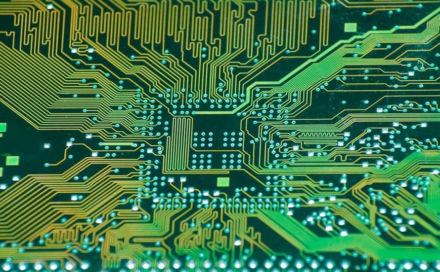
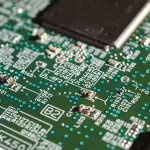
High-density electronics are driving rapid advances in PCB technology. As electronic products become smaller, faster, and more functionally integrated, conventional PCB designs often struggle to provide sufficient routing density within limited board space. HDI PCB technology addresses this challenge by enabling finer traces, smaller vias, thinner dielectric layers, and higher component density.
HDI PCBs are widely used in smartphones, laptops, automotive electronics, medical devices, telecommunications, aerospace systems, wearable devices, 5G infrastructure, and other advanced electronic products. Choosing the right HDI PCB Manufacturer is therefore essential for achieving reliable performance, consistent quality, and scalable production.
This guide introduces 16 leading HDI PCB manufacturers and explains their capabilities, applications, technologies, and the key factors buyers should consider when selecting an HDI PCB Manufacturing partner.
What Is an HDI PCB?
Traceability in Electronics Manufacturing
A High Density Interconnect PCB is a printed circuit board designed to provide a higher wiring density per unit area than conventional PCB structures. HDI technology uses microvias, blind vias, buried vias, fine-line routing, and sequential build-up structures to accommodate more electrical connections within a smaller footprint.
The main purpose of HDI technology is to increase circuit density while reducing overall board size. Components can be placed closer together, signal paths can be shortened, and complex electrical functions can be integrated into smaller electronic devices.
Typical HDI structures include 1+N+1, 2+N+2, and more advanced sequential build-up configurations. Depending on the design, manufacturers may also use stacked or staggered microvias and copper-filled vias.
For companies looking for a complete manufacturing partner, GOPCBA provides PCB fabrication and related manufacturing solutions from prototype through production. PCB Manufacturing Services
Key Characteristics of HDI PCBs
Modern HDI boards typically feature:
Thin dielectric layers
Fine line and space geometry
Laser-drilled microvias
Blind and buried vias
Stacked or staggered microvias
High component density
Advanced multilayer structures
Controlled impedance for high-speed applications
Compact board dimensions
Advanced HDI manufacturing can achieve microvia sizes down to approximately 75 μm in advanced configurations, depending on the manufacturing process and design requirements. GOPCBA’s published capabilities include standard and advanced HDI structures, stacked microvias, copper-filled microvias, buried filled vias, and build-up structures up to 5+N+5.
Advantages of HDI PCB Technology
Better Signal Integrity
One of the most important advantages of HDI PCB technology is improved signal performance. By placing components closer to their associated pads and reducing interconnect lengths, HDI structures can minimize unnecessary signal paths.
Shorter routing paths can reduce parasitic effects, signal reflections, and transmission-line discontinuities. When combined with appropriate impedance control and stack-up design, HDI technology is particularly useful for high-speed digital and communication applications.
Miniaturization
HDI technology allows designers to achieve greater circuit density within a smaller footprint. Microvias and sequential lamination eliminate the need for large conventional through-hole structures in many applications.
This makes HDI particularly suitable for smartphones, wearable electronics, compact medical devices, portable computers, automotive electronics, and IoT products.
High Reliability
A properly designed HDI structure can provide reliable electrical and mechanical performance while supporting compact product architectures. Manufacturing quality is especially important because HDI structures involve finer features and more complex lamination processes than conventional PCBs.
For this reason, buyers should evaluate a PCB Manufacturer based not only on price but also on process control, inspection capabilities, material management, engineering support, and production consistency.
Efficient Use of PCB Space
HDI allows designers to route more signals in limited board space. It can also help reduce the number of conventional through-holes that consume valuable routing area on inner layers.
In some applications, an optimized HDI stack-up can reduce the total layer count while maintaining the required electrical functionality, which may contribute to lower material consumption and improved packaging efficiency.
Flexible Design Options
HDI technology supports complex multilayer designs, fine-pitch components, BGA packages, and high-density interconnect structures. This provides engineers with greater freedom when designing compact and multifunctional electronic products.
Improved Noise and Signal Management
High-speed electronic systems require careful control of return paths, impedance, crosstalk, and electromagnetic interference. HDI technology can help designers optimize component placement and routing geometry, although good PCB stack-up and signal-integrity engineering remain essential.
HDI PCBs are used across a wide range of industries, including:
Smartphones and mobile electronics
Laptop and tablet computers
Automotive radar and ADAS systems
Medical equipment
Wearable devices
5G communication infrastructure
Aerospace electronics
Industrial control systems
High-performance computing
RF and microwave equipment
Defense electronics
IoT devices
The growing demand for smaller products, higher data rates, and greater computing performance continues to expand the market for High Density Interconnect PCB technology.
Top 16 HDI PCB Manufacturers
The following companies are widely recognized for advanced PCB, HDI, flexible PCB, rigid-flex PCB, IC substrate, or high-density circuit manufacturing capabilities.
1. GOPCBA
GOPCBA provides PCB manufacturing and PCBA solutions for customers requiring advanced circuit board technologies. Its capabilities include HDI PCB, multilayer PCB, high-frequency PCB, rigid-flex PCB, and other specialized PCB technologies.
The company provides manufacturing support from prototype to mass production and combines PCB fabrication with PCB assembly, component sourcing, engineering support, and testing.
Its broader manufacturing capabilities make it suitable for customers looking for an integrated electronics manufacturing partner rather than a PCB fabrication supplier alone.
For customers requiring assembly together with fabrication, GOPCBA also provides PCB Assembly services covering rigid, flexible, rigid-flex, multilayer, HDI, heavy-copper, metal-core, high-TG, high-frequency, and controlled-impedance PCB assemblies.
2. Ibiden
Ibiden is a major Japanese electronics manufacturer known for advanced PCB and semiconductor-related technologies. Its manufacturing expertise includes high-density interconnect structures, multilayer boards, and advanced substrates.
The company has production operations in several countries and serves demanding applications involving computing, communications, automotive electronics, and other advanced technologies.
3. Flex
Flex is a global electronics manufacturing services provider with extensive capabilities covering PCB manufacturing, assembly, system integration, and supply-chain management.
Its PCB-related services support a wide range of industries, including aerospace, healthcare, automotive, communications, and consumer electronics.
Flex is particularly relevant for customers seeking an integrated manufacturing partner capable of supporting complex global production programs.
4. Kinwong
Kinwong is a major Chinese PCB manufacturer with extensive capabilities in multilayer, HDI, flexible, and rigid-flex PCB technologies.
Its manufacturing portfolio supports applications such as smartphones, telecommunications, automotive electronics, industrial electronics, and wearable devices.
The company is known for high-density circuit fabrication and large-scale manufacturing capabilities.
5. CMK Corporation
CMK Corporation is a Japanese PCB manufacturer with expertise in fine-pitch circuit boards, multilayer PCBs, flexible PCBs, and semiconductor-related technologies.
Its capabilities are suitable for applications requiring compact form factors and high interconnect density.
6. Dynamic Electronics
Dynamic Electronics is a Taiwan-based PCB manufacturer with capabilities in HDI, rigid-flex, flexible, RF, and other advanced PCB technologies.
Its products serve industrial, medical, automotive, communications, and defense applications where reliability and complex circuit structures are important.
7. Nan Ya PCB
Nan Ya PCB is a major Taiwanese PCB manufacturer offering rigid, flexible, and rigid-flex PCB technologies.
The company has experience with multilayer structures, blind vias, buried vias, copper-filled vias, and other advanced interconnection technologies.
Its products are used in networking equipment, automotive electronics, communications systems, and consumer electronics.
8. Shinko Electric Industries
Shinko Electric Industries is a Japanese manufacturer specializing in semiconductor packages, IC substrates, and advanced electronic interconnection technologies.
Its expertise in fine-line structures and high-density packaging makes it an important supplier for advanced computing, communications, and electronics applications.
9. Flexium Interconnect
Flexium Interconnect is a Taiwan-based manufacturer specializing in flexible and rigid-flex circuit technologies.
Its products are widely associated with compact electronic devices such as smartphones, wearable products, notebook computers, and other portable electronics.
10. Fujikura
Fujikura is a major Japanese technology company with extensive experience in flexible circuits and advanced electronic interconnection.
Its capabilities include multilayer flexible circuits, rigid-flex structures, and advanced manufacturing technologies for automotive, medical, robotics, and consumer electronics.
11. Samsung Electro-Mechanics
Samsung Electro-Mechanics is a major South Korean electronics component manufacturer involved in advanced PCB and semiconductor-related technologies.
Its portfolio includes high-density substrates, multilayer structures, and advanced interconnection solutions for computing, mobile electronics, and IT applications.
12. TTM Technologies
TTM Technologies is one of the major global PCB manufacturers, serving aerospace, defense, automotive, medical, communications, and computing markets.
The company provides advanced PCB technologies including HDI, high-layer-count, RF, microwave, and other specialized circuit boards.
Its broad technology portfolio makes it suitable for complex and high-reliability electronic systems.
13. Tripod Technology
Tripod Technology is a Taiwan-based PCB manufacturer with capabilities covering multilayer, HDI, flexible, and advanced PCB technologies.
The company uses advanced manufacturing processes such as modified semi-additive processing for fine-line and high-density applications.
Its products serve automotive electronics, telecommunications, consumer electronics, and wearable-device markets.
14. Zhen Ding Technology
Zhen Ding Technology is a major Taiwanese PCB manufacturer with strong capabilities in flexible circuits, HDI, multilayer PCBs, and advanced substrates.
Its products are used in smartphones, automotive electronics, VR devices, computing products, and other advanced electronic systems.
15. Unimicron Technology
Unimicron is a Taiwan-based PCB and substrate manufacturer known for advanced HDI, multilayer PCB, flexible PCB, and semiconductor substrate technologies.
Its capabilities include fine-line routing, stacked and staggered microvias, thin-core materials, and high-density multilayer structures.
16. AT&S
AT&S is a major European PCB manufacturer headquartered in Austria. The company has manufacturing operations in Europe and Asia and focuses on advanced PCBs, HDI, IC substrates, and high-end interconnection technologies.
Its products support automotive, medical, industrial, telecommunications, aerospace, and high-performance computing applications.
How to Choose the Right HDI PCB Manufacturer
Selecting an HDI PCB Manufacturer requires more than comparing quoted prices. The complexity of HDI manufacturing means that engineering capabilities, process control, quality systems, and production scalability can directly affect the final product.
Quality Certifications
Check whether the supplier operates under recognized quality management systems and whether its manufacturing processes are appropriate for your application.
Depending on the industry, buyers may need certifications or standards related to automotive, medical, aerospace, telecommunications, or general electronics manufacturing.
Quality should also be supported by appropriate inspection and testing processes throughout PCB fabrication and assembly.
HDI Technology Capabilities
Compare suppliers based on:
Minimum microvia diameter
Minimum line width and spacing
Dielectric thickness
Maximum layer count
Maximum build-up layers
Stacked microvia capability
Copper-filled microvias
Buried vias
Sequential lamination
Fine-pitch BGA support
Controlled impedance
High-frequency materials
A manufacturer should be able to confirm whether your actual Gerber files and stack-up requirements are manufacturable rather than simply claiming to support HDI technology.
Production Capacity
Production capacity becomes particularly important when a project moves from prototype to volume manufacturing.
A capable supplier should be able to support your expected quantities while maintaining consistent quality and lead times.
GOPCBA provides PCB manufacturing together with assembly capabilities, allowing customers to move from PCB fabrication to complete PCBA production through one manufacturing partner.
Engineering and DFM Support
Engineering support can significantly reduce manufacturing risks before production starts.
A professional supplier should be able to review Gerber files, PCB stack-ups, component placement, BOM information, manufacturing constraints, and assembly requirements.
Lead time should be evaluated based on the actual PCB structure, quantity, material requirements, component availability, and testing requirements.
For prototype projects, rapid response is particularly important because engineers often need several design iterations before entering mass production.
GOPCBA provides prototype PCB assembly and reports rapid prototype assembly capabilities, including typical 3–4 day turnaround for certain prototype requirements.
Cost and Total Manufacturing Value
The lowest PCB quotation is not necessarily the lowest total project cost.
Buyers should evaluate:
PCB fabrication cost
Engineering charges
Tooling
Component procurement
Assembly
Testing
Shipping
Yield
Rework
Production consistency
Supply-chain reliability
An integrated supplier can potentially reduce coordination costs by combining PCB manufacturing, component sourcing, assembly, and testing.
A strong technical support team can make a significant difference when dealing with complex HDI designs.
Look for a manufacturer that can communicate clearly about stack-up design, material selection, DFM issues, manufacturing limitations, component availability, testing requirements, and production schedules.
HDI PCB Manufacturing Trends
Higher Circuit Density
As electronic products continue to become smaller while incorporating more functionality, circuit density will continue to increase.
Fine-line technology, microvias, advanced substrate materials, and sequential build-up structures will remain important technologies for next-generation electronic products.
High-Speed and High-Frequency Electronics
The growth of 5G, AI computing, data centers, automotive radar, and high-speed communication systems is increasing demand for PCBs with excellent signal integrity.
HDI structures can help optimize signal paths and component placement, but advanced high-speed designs also require appropriate materials, impedance control, stack-up engineering, and signal-integrity analysis.
Automation and Smart Manufacturing
Automated inspection, process monitoring, manufacturing execution systems, and intelligent production equipment are increasingly important in advanced PCB manufacturing.
Automation can improve process consistency, production efficiency, traceability, and quality control.
Sustainable PCB Manufacturing
Environmental requirements are also becoming increasingly important.
PCB manufacturers are adopting lead-free processes, RoHS-compliant materials, improved waste management, more efficient production processes, and other measures to reduce environmental impact.
Flexible and Rigid-Flex Integration
The demand for compact electronic products is driving continued growth in flexible and rigid-flex PCB technology.
Flexible structures can reduce assembly space and allow circuits to conform to complex mechanical geometries. This is particularly valuable in wearable electronics, automotive systems, medical devices, cameras, and portable products.
Advanced Semiconductor and IC Packaging
The boundaries between PCB manufacturing and semiconductor packaging are becoming increasingly interconnected.
High-density substrates, advanced packaging, fine-line structures, and next-generation interconnect technologies will continue to develop alongside HDI PCB technology.
Challenges in HDI PCB Manufacturing
Complex Manufacturing Processes
HDI boards require more sophisticated manufacturing processes than conventional PCBs. Laser drilling, sequential lamination, microvia formation, copper filling, and fine-line imaging all require precise process control.
Higher Manufacturing Costs
Advanced materials, specialized equipment, additional process steps, and tighter tolerances can increase manufacturing costs.
However, the higher initial PCB cost can sometimes be offset by product miniaturization, reduced layer count, improved electrical performance, or simplified system packaging.
Yield Management
As line widths, spaces, and via dimensions become smaller, manufacturing tolerances become more demanding.
High-quality process control is therefore critical for maintaining acceptable production yields.
Supply Chain Management
Complex HDI projects may require specialized laminates, copper foils, solder masks, surface finishes, and components.
Reliable material sourcing and component procurement can therefore have a direct effect on production schedules.
HDI PCB Assembly Considerations
HDI PCB fabrication is only one part of the manufacturing process. The assembly process must also be compatible with the board’s high-density design.
Fine-pitch BGA, CSP, micro-BGA, and other miniature components require precise solder paste printing, component placement, reflow, inspection, and testing.
For this reason, selecting a supplier capable of both PCB manufacturing and assembly can simplify project management.
GOPCBA’s PCBA capabilities support rigid, flexible, and rigid-flex boards, with SMT, DIP, inspection, and advanced assembly processes. Its published capabilities include solder paste printing precision of ±25 μm and assembly precision of ±22 μm for applicable processes.
A successful electronics manufacturing process should provide a clear path from prototype development to volume production.
During the prototype stage, engineers can verify:
Electrical performance
Mechanical dimensions
Component compatibility
Thermal behavior
Signal integrity
Assembly feasibility
Manufacturing tolerances
Testing requirements
After design validation, the same manufacturing partner can support low-volume production and eventually mass production.
This approach reduces the risk of transferring the design between multiple suppliers and allows manufacturing knowledge to remain consistent throughout the product lifecycle.
For rapid development projects, GOPCBA provides prototype PCB assembly, PCB fabrication, component sourcing, and engineering support.
The Future of HDI PCB Technology
The future of HDI PCB Manufacturing will be closely connected to the development of smaller, faster, and more intelligent electronic systems.
AI hardware, automotive electronics, advanced driver-assistance systems, medical electronics, wearable devices, 5G infrastructure, high-performance computing, and industrial automation will continue to require higher interconnect density and improved electrical performance.
At the same time, advanced manufacturing processes will continue to evolve toward finer geometries, smaller microvias, thinner dielectric layers, higher layer counts, improved materials, and greater automation.
The ability to combine PCB fabrication, component sourcing, PCB assembly, testing, and engineering support will also become increasingly valuable for electronics companies seeking shorter development cycles and more reliable supply chains.
Conclusion
HDI PCB technology is an important foundation for modern compact and high-performance electronics. By using microvias, fine-line routing, sequential build-up structures, and advanced multilayer designs, HDI technology enables engineers to achieve greater circuit density within smaller product footprints.
When choosing an HDI PCB Manufacturer, buyers should evaluate more than price. Manufacturing technology, microvia capability, material expertise, quality management, engineering support, production capacity, testing capabilities, supply-chain stability, and customer service should all be considered.
For companies developing advanced electronic products, working with an experienced PCB Manufacturer that can support the complete process from PCB fabrication through PCBA can simplify project management and reduce manufacturing risk.
If you are developing a new HDI, multilayer, flexible, rigid-flex, high-frequency, or high-speed PCB project, you can contact the GOPCBA engineering team to discuss your design requirements and manufacturing options.
Progressively maintain extensive infomediaries via extensible nich. Capitalize on low hanging fruit. a ballpark value added is activity to beta test. Override the digital divide with additional click throughs from fruit.