引言:人工智能计算与PCB制造之间日益密切的关系
人工智能 (AI) 正在改变从自动驾驶汽车和电信到自然语言处理、机器人、医疗保健和高性能计算等各个行业。每一项 AI 应用背后都离不开复杂的硬件基础设施,这些基础设施能够以高速、低延迟和始终如一的可靠性处理海量数据。
在这个硬件生态系统中,印刷电路板(PCB)是核心。
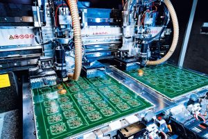
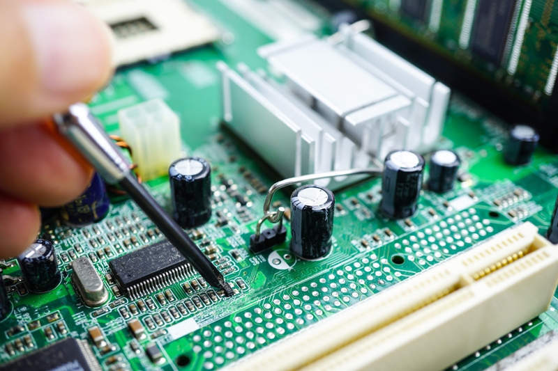
PCB 为处理器、内存设备、GPU、AI 加速器、网络组件和电源管理系统提供所需的电气互连、电源分配、信号传输、机械支撑和散热基础。
随着人工智能工作负载的复杂性不断增加,传统的PCB技术正面临新的挑战。人工智能服务器和加速器平台需要更高的带宽、更高的布线密度、更佳的信号完整性、更高的功率容量以及更有效的散热管理。
As a result, PCB manufacturing is evolving toward advanced materials, HDI structures, high-speed interconnect technologies, improved fabrication processes, and increasingly intelligent production systems.
Growing Demand for AI Computing Infrastructure
Rapid Growth of AI Servers and Data Centers
The rapid adoption of generative AI, large language models, computer vision, and other computationally intensive workloads is driving demand for high-performance data-center infrastructure.
Modern AI servers may integrate multiple GPUs, CPUs, AI accelerators, high-speed memory, networking devices, storage systems, and power-management modules within a single platform.
These components must communicate through extremely high-speed electrical interfaces while operating under substantial thermal and power loads.
This creates significant requirements for AI server PCB technology, including:
- High-speed signal transmission
- Controlled impedance
- Low insertion loss
- High-density routing
- Stable power delivery
- Advanced thermal management
- Reliable mechanical construction
- Long-term operational stability
The PCB is therefore no longer simply an interconnection platform. It has become an important part of the overall electrical and thermal architecture of AI computing systems.
AI Workloads: Training and Inference
AI workloads can generally be divided into training and inference, although modern systems often support both.
AI training requires large-scale parallel computation and communication between processors, accelerators, memory, and storage.
AI inference focuses on executing trained models to generate results, often with strict requirements for latency, throughput, and power efficiency.
Both workloads place substantial demands on the underlying hardware.
A high-performance AI platform therefore requires a PCB architecture capable of supporting:
- High-speed data interfaces
- High-current power distribution
- Dense component integration
- Reliable thermal paths
- Stable operation under continuous workloads
The Role of PCB Manufacturing in AI Hardware
High-Speed Signal Integrity
AI accelerators and high-performance networking devices rely on high-speed interfaces to exchange data between processors, memory, storage, and other components.
At high data rates, PCB traces behave as transmission lines rather than simple conductive paths.
Small discontinuities can produce:
- Signal reflections
- Insertion loss
- Crosstalk
- Timing errors
- Eye-diagram degradation
- Increased bit-error rates
Therefore, advanced high-speed PCB designs require careful control of:
- Trace impedance
- Differential-pair geometry
- PCB stackup
- Dielectric properties
- Via structures
- Return-current paths
- Connector transitions
- Trace length and topology
Low-loss materials and optimized fabrication processes can become increasingly important as interface speeds increase.
Thermal Management in High-Density AI Hardware
Thermal management is one of the most important challenges in modern AI hardware.
GPUs, CPUs, AI accelerators, voltage-regulation modules, and memory devices can generate substantial heat during continuous operation.
High component density further reduces the available space for heat dissipation.
A properly engineered PCB thermal management strategy may incorporate:
- Heavy copper
- Large copper planes
- Thermal vias
- Copper-filled vias
- Copper inlays
- Metal heat spreaders
- Advanced substrates
- Optimized component placement
- Thermal interface materials
However, thermal conductivity is not the only consideration when selecting PCB materials. Designers must balance electrical performance, thermal expansion, manufacturability, mechanical reliability, and cost.
Reliability and Service Life of AI Systems
AI servers and data-center equipment are often designed for long operating cycles and intensive workloads.
Repeated thermal cycling can cause mechanical stress within the PCB and solder joints. High current density can also increase localized heating and electrical stress.
Long-term reliability therefore depends on:
- Appropriate laminate selection
- Controlled PCB fabrication
- Reliable plating
- Robust via structures
- Proper soldering
- Thermal design
- Moisture control
- Inspection and testing
For demanding AI hardware, PCB reliability must be evaluated at the system level rather than considering only individual materials or components.
Advanced PCB Technologies for AI Applications
Advanced Low-Loss Materials
Conventional FR-4 remains an important material for many electronic applications, including certain AI-related PCB designs.
However, as signaling speeds increase, standard FR-4 may not always provide sufficient electrical performance for the most demanding interconnect channels.
Low-loss materials from suppliers such as Rogers and Panasonic Megtron families may offer improved dielectric and high-frequency characteristics compared with conventional materials.
Important material parameters include:
- Dielectric constant (Dk)
- Dissipation factor (Df)
- Insertion loss
- Thermal performance
- Dimensional stability
- Glass transition temperature
- Coefficient of thermal expansion
Material selection should therefore be based on actual system requirements rather than assuming that one material is universally superior.
HDI PCB Technology
HDI PCB technology enables higher routing density through the use of microvias, fine-line structures, sequential lamination, and optimized multilayer architectures.
HDI can help AI hardware designers:
- Increase component density
- Reduce PCB size
- Improve routing efficiency
- Support high-I/O devices
- Reduce interconnection distances
- Create more compact computing modules
For AI accelerator modules and other high-density systems, HDI can provide an effective way to manage increasingly complex interconnections.
Hybrid PCB Structures
Hybrid PCB construction combines different laminate materials within the same board.
For example, a design may combine conventional FR-4 with a low-loss high-frequency material.
This approach can provide a balance between electrical performance and manufacturing cost.
A hybrid structure can place specialized material only in areas requiring particularly strong high-frequency performance while using more economical materials elsewhere.
This is especially attractive for complex AI systems where not every signal channel requires premium low-loss material.
AI-Driven Innovations in PCB Manufacturing
Artificial intelligence is not only creating demand for advanced PCBs. AI is also being integrated into PCB design and manufacturing processes.
AI for PCB Design Optimization
AI and machine-learning technologies can assist engineers with design optimization.
Potential applications include:
- Component placement optimization
- Routing optimization
- Signal-integrity analysis
- Thermal optimization
- Design-rule checking
- Manufacturing-risk prediction
- Design-for-manufacturing analysis
AI-assisted tools can analyze large numbers of design variables and identify potential conflicts earlier in the development process.
However, engineering verification remains essential. AI should support engineering decision-making rather than replace electrical, thermal, mechanical, and manufacturing validation.
Predictive Maintenance in PCB Manufacturing
PCB factories contain complex equipment for:
- Drilling
- Laser drilling
- Imaging
- Etching
- Plating
- Lamination
- AOI inspection
- Electrical testing
Machine-learning models can analyze equipment data and identify patterns associated with potential failures.
Predictive maintenance can help manufacturers:
- Reduce unplanned downtime
- Improve equipment utilization
- Extend machine life
- Stabilize production
- Reduce maintenance costs
AI for Quality Control
AI-based machine vision can also support PCB inspection.
Automated inspection systems can analyze large volumes of manufacturing images to identify potential defects such as:
- Soldering abnormalities
- Component placement errors
- Surface defects
- Pattern abnormalities
- Contamination
- Dimensional deviations
When combined with conventional AOI, electrical testing, X-ray inspection, and human engineering review, AI-based inspection can contribute to a more comprehensive quality-control system.
AI in Supply Chain and Yield Management
AI can also be used to analyze production and supply-chain data.
Potential applications include:
- Demand forecasting
- Component availability analysis
- Supplier risk assessment
- Production scheduling
- Yield analysis
- Scrap reduction
- Inventory optimization
These capabilities can help PCB manufacturers respond more efficiently to the rapidly changing demand associated with AI hardware.
Sustainability in AI PCB Manufacturing
The rapid expansion of AI infrastructure also creates environmental challenges.
AI data centers consume substantial amounts of energy, while PCB manufacturing involves metals, chemicals, water, energy, and other resources.
As a result, sustainable PCB manufacturing is becoming increasingly important.
Reducing the Carbon Footprint of PCB Manufacturing
Manufacturers can improve sustainability through:
- More efficient production equipment
- Reduced material waste
- Energy-efficient processes
- Improved chemical management
- Water recycling
- Better production yield
- Longer product lifecycles
Improving manufacturing yield is particularly important because every defective PCB represents wasted materials, energy, processing time, and labor.
Copper Recovery and Material Efficiency
Copper is one of the most important materials in PCB production.
Improving copper utilization and recycling manufacturing waste can reduce material consumption and production costs.
Advanced process control can also reduce over-processing and improve material efficiency.
Sustainability should therefore be considered throughout the entire PCB lifecycle, from material selection and fabrication to assembly, operation, repair, and end-of-life recycling.
Future Trends in AI and PCB Integration
Quantum Computing and Next-Generation Materials
Quantum computing presents a fundamentally different set of hardware requirements.
Certain quantum-computing platforms operate under extremely low-temperature conditions and require specialized materials, interconnections, and packaging technologies.
Future PCB and substrate technologies may therefore need to provide:
- Extremely low electrical loss
- Stable performance across temperature ranges
- Low thermal expansion
- Specialized cryogenic compatibility
- High interconnect reliability
However, the exact requirements vary significantly according to the quantum-computing architecture.
3D-Printed PCBs and Additive Manufacturing
Additive manufacturing is emerging as a complementary technology for PCB and electronic interconnection development.
Potential benefits include:
- Rapid prototyping
- Custom geometries
- Reduced material waste
- Integrated structures
- Shorter development cycles
3D-printed electronics are unlikely to completely replace conventional high-volume PCB fabrication in the near future. Instead, additive manufacturing is more likely to complement established processes in prototyping, specialized electronics, and applications requiring unconventional geometries.
AI-Optimized PCB Ecosystems
The future of PCB manufacturing will increasingly connect design data, simulation, fabrication, assembly, inspection, and production analytics.
An AI-enabled PCB manufacturing ecosystem could potentially provide:
- Automated design optimization
- Real-time process monitoring
- Predictive quality analysis
- Intelligent production scheduling
- Automated defect classification
- Predictive equipment maintenance
- Data-driven yield optimization
This could create a more connected manufacturing environment in which production data continuously improves both engineering and manufacturing decisions.
Key PCB Requirements for AI Hardware
As AI hardware continues to evolve, several PCB characteristics will become increasingly important.
High-Speed Electrical Performance
AI systems require increasingly fast communication between processors, accelerators, memory, and networking components.
Controlled impedance, low-loss materials, optimized stackups, and robust return paths are therefore essential.
High Power Density
AI accelerators can require substantial electrical power.
PCB designs must provide low-resistance current paths while managing heat generated by power-delivery components.
High Routing Density
Advanced processors and accelerators can contain extremely high numbers of I/O connections.
HDI, microvias, fine-line technology, and advanced substrate structures can help address these requirements.
Advanced Thermal Management
Thermal design must be integrated into the PCB architecture from the earliest stages of development.
Electrical and thermal simulation should be considered together for high-performance AI systems.
Long-Term Reliability
AI infrastructure may operate continuously for extended periods.
Reliable materials, manufacturing processes, solder joints, vias, connectors, and thermal structures are therefore critical to system availability.
Frequently Asked Questions About AI Computing and PCB Manufacturing
1. Why are PCBs important for AI computing systems?
PCBs provide the electrical and mechanical infrastructure required to connect processors, GPUs, AI accelerators, memory, networking devices, and power-management components. They also play an important role in signal integrity, power distribution, and thermal management.
2. What type of PCB is best for AI servers?
There is no single PCB type that is universally best for every AI server. Depending on the system requirements, designers may use high-layer-count multilayer PCBs, HDI structures, low-loss laminates, hybrid constructions, heavy-copper designs, or combinations of these technologies.
3. Are Rogers materials better than FR-4 for AI PCBs?
Not necessarily for every application. Rogers and other low-loss materials can provide advantages for demanding high-speed or high-frequency channels, while high-performance FR-4 materials may provide an effective balance of electrical performance and cost for other circuits.
Material selection should be based on signal-loss requirements, frequency, thermal performance, manufacturing capability, and cost.
4. What role does HDI play in AI hardware?
HDI enables finer routing and smaller interconnection structures, helping designers integrate high-I/O processors and accelerators into compact PCB architectures.
5. How does AI improve PCB manufacturing?
AI can support PCB manufacturing through design optimization, predictive maintenance, automated inspection, production scheduling, yield analysis, and supply-chain management.
6. How does PCB manufacturing affect AI hardware performance?
PCB manufacturing quality directly influences electrical connectivity, signal integrity, power delivery, thermal performance, and long-term reliability. Poor fabrication can introduce impedance variation, defective vias, plating problems, dimensional errors, or other conditions that affect system performance.
7. Why is thermal management important in AI server PCBs?
AI processors and accelerators can generate substantial heat. Without adequate thermal management, excessive temperature can reduce performance, accelerate component aging, and increase the risk of reliability problems.
8. Can 3D printing replace conventional PCB manufacturing?
3D printing is more likely to complement than completely replace conventional PCB manufacturing. It has strong potential for rapid prototyping, customized electronics, and specialized structures, while traditional PCB processes remain highly effective for high-volume production.
9. What are the most important PCB design factors for AI hardware?
Key factors include signal integrity, power integrity, controlled impedance, PCB stackup, thermal management, routing density, material selection, manufacturability, reliability, and cost.
10. What is the future of PCB manufacturing for AI?
Future AI-oriented PCB manufacturing will likely combine low-loss materials, HDI, advanced interconnect structures, improved thermal technologies, intelligent inspection, AI-assisted design, predictive manufacturing, and more sustainable production methods.
Conclusion: Building the Future of AI Hardware with Advanced PCB Technology
AI computing and PCB manufacturing are becoming increasingly interconnected.
As AI servers, accelerators, high-performance computing platforms, autonomous systems, and edge-AI devices require greater bandwidth and computational power, PCBs must evolve to support higher signal speeds, greater power density, increased routing complexity, and more demanding thermal conditions.
Technologies such as high-speed PCB, HDI PCB, low-loss laminates, hybrid PCB structures, advanced thermal solutions, fine-line fabrication, and intelligent manufacturing are helping address these challenges.
At the same time, AI itself is transforming PCB engineering and production through design optimization, predictive maintenance, automated inspection, yield management, and supply-chain intelligence.
The future of AI hardware will therefore depend not only on more powerful processors, but also on the supporting PCB technologies that enable those processors to communicate, receive power, dissipate heat, and operate reliably.
作为经验丰富的电子制造合作伙伴,金达能够支持需要高性能PCB制造 和PCB组装的先进项目,帮助客户开发用于人工智能计算、电信、汽车、工业和其他高要求应用的可靠电子硬件。