As the electronics industry continues to expand, sustainability has become an increasingly important consideration in PCB manufacturing and PCB assembly. The rapid growth of consumer electronics, electric vehicles, medical devices, IoT products, AI hardware, and industrial electronics has also increased demand for raw materials, energy, and electronic manufacturing resources.
As a result, manufacturers are exploring ways to reduce the environmental impact of electronic products without compromising electrical performance, reliability, safety, or manufacturing efficiency.
This has accelerated interest in green materials in PCB assembly, including biodegradable PCB substrate materials, paper PCB substrates, cellulose PCB substrates, sustainable PCB laminates, eco-friendly PCB coatings, and water-based PCB inks.
However, sustainable electronics manufacturing is not simply a matter of replacing one material with another. Engineers must evaluate the complete product lifecycle, including material sourcing, PCB fabrication, assembly processes, energy consumption, component selection, product reliability, recyclability, and end-of-life handling.
For this reason, the future of sustainable PCB assembly depends on balancing environmental responsibility with engineering performance.
Why Green Materials Matter in PCB Assembly
Traditional PCB materials such as conventional FR-4 laminates provide excellent electrical insulation, mechanical strength, thermal stability, and manufacturability. However, many conventional PCB structures rely on fiberglass, thermoset resins, copper, solder, coatings, and chemical processing steps that can make end-of-life recycling and material recovery more difficult.
At the same time, the electronics industry is facing increasing pressure to reduce:
- Material waste
- Hazardous substances
- VOC emissions
- Manufacturing energy consumption
- Water consumption
- Carbon emissions
- Electronic waste
- Difficult-to-recycle materials
This is driving interest in eco-friendly PCB manufacturing and sustainable PCB assembly.
Green materials can contribute to sustainability in several ways:
Lower environmental impact: Bio-based or recyclable materials may reduce dependence on petroleum-derived resources.
Reduced hazardous substances: Lead-free soldering and compliant materials can reduce exposure to restricted substances.
Improved recyclability: Materials designed for easier separation or recovery can support circular-economy strategies.
Lower emissions: Water-based coatings and inks can reduce reliance on solvent-intensive processes.
Improved resource efficiency: Better material utilization and manufacturing process control can reduce waste.
It is important to note that “green” does not automatically mean “better” for every application. Material selection must always consider electrical, thermal, mechanical, environmental, and lifecycle requirements.
What Are Biodegradable PCB Substrate Materials?
The PCB substrate is the structural foundation that supports conductive copper layers and provides electrical insulation between circuits.
Conventional FR-4 is a thermoset composite based on fiberglass and epoxy resin. It is widely used because of its excellent mechanical and electrical properties, but it is not designed to biodegrade naturally.
Biodegradable PCB substrate materials seek to address this limitation by incorporating renewable or biodegradable materials into the substrate structure.
Potential material families include:
- Plant-based polymers
- Bio-based resins
- Cellulose-based materials
- Natural-fiber composites
- Biodegradable polymer systems
- Recyclable thermoplastic substrates
These materials are particularly interesting for products designed for short lifecycles, temporary sensing, disposable electronics, educational electronics, and environmentally sensitive applications.
However, biodegradable substrates still have technical limitations compared with mature PCB materials. Engineers need to evaluate:
- Moisture absorption
- Thermal stability
- Mechanical strength
- Dimensional stability
- Dielectric properties
- Soldering compatibility
- Storage life
- Manufacturing process compatibility
For high-temperature, high-frequency, automotive, aerospace, or medical applications, conventional high-performance materials may remain more appropriate.
Paper PCB Substrate: A Lightweight Sustainable Option
The paper PCB substrate concept uses paper or cellulose-based structures as an alternative substrate for selected electronic applications.
Paper-based electronics provide several attractive characteristics:
- Lightweight construction
- Renewable feedstock
- Low material cost
- Potential recyclability
- Simple disposal
- Compatibility with low-cost printed electronics
Paper substrates can be useful for low-power electronics and environmentally focused applications where extreme thermal and mechanical performance is not required.
Potential applications include:
- Educational electronics
- Disposable sensors
- Smart packaging
- RFID-related applications
- Low-power IoT devices
- Temporary electronic systems
However, paper is naturally sensitive to moisture and mechanical deformation. Therefore, protective coatings or encapsulation may be required.
Paper-based PCB technology should therefore be evaluated based on actual application requirements rather than treated as a universal replacement for FR-4.
Cellulose PCB Substrate: Combining Renewable Materials with Electronics
A cellulose PCB substrate uses cellulose or cellulose-derived materials as part of its structural system.
Cellulose is attractive because it is:
- Renewable
- Widely available
- Lightweight
- Potentially biodegradable
- Suitable for composite material development
Researchers are investigating nanocellulose, cellulose nanofibers, and lignocellulosic materials for flexible and sustainable electronics.
Potential applications include:
- Flexible sensors
- Wearable electronics
- Disposable electronics
- Smart packaging
- Low-power IoT devices
The primary challenge is environmental stability.
Cellulose-based materials may have greater sensitivity to:
- Humidity
- Water absorption
- Temperature
- Dimensional changes
Therefore, cellulose PCB substrates often require protective coatings or hybrid material structures when exposed to demanding environments.
Sustainable PCB Laminates
The development of sustainable PCB laminates is one of the most important areas in environmentally responsible PCB manufacturing.
Traditional PCB laminates are optimized for electrical performance and mechanical reliability. New sustainable laminate technologies aim to incorporate:
- Bio-based resins
- Recycled materials
- Halogen-free systems
- Renewable reinforcement materials
- Lower-impact resin systems
- Recyclable thermoplastic structures
Bio-Based PCB Laminates
Bio-based laminates may use renewable feedstocks to partially replace petroleum-derived resin components.
The sustainability advantage depends on factors such as:
- Renewable content
- Manufacturing energy
- Resin chemistry
- Product lifetime
- End-of-life treatment
A bio-based material with poor reliability may ultimately create more waste if products fail prematurely. Therefore, lifecycle performance is more important than simply maximizing bio-based content.
Halogen-Free PCB Materials
Halogen-free PCB materials are another important component of environmentally conscious PCB manufacturing.
Halogen-free materials can help manufacturers meet customer and regulatory requirements while reducing dependence on certain halogenated flame-retardant systems.
For many commercial and industrial electronics products, halogen-free laminates can provide a practical balance between:
Environmental compliance + electrical performance + thermal reliability + manufacturability
Eco-Friendly PCB Coatings
PCB coatings protect electronic assemblies from environmental stress.
Typical PCB protection systems include:
- Conformal coatings
- Protective varnishes
- Encapsulation materials
- Potting compounds
- Protective surface treatments
Traditional coating systems may use solvent-based chemistry, which can generate VOC emissions during manufacturing.
Eco-friendly PCB coatings increasingly use:
- Water-based formulations
- Low-VOC chemistry
- Bio-derived resins
- Solvent-reduced systems
These technologies can reduce environmental impact while protecting PCBs from:
- Moisture
- Dust
- Chemicals
- Corrosion
- Condensation
- Salt contamination
However, engineers must compare coating systems based on actual requirements.
Important parameters include:
- Dielectric strength
- Adhesion
- Moisture resistance
- Chemical resistance
- Temperature range
- UV stability
- Reworkability
- Curing characteristics
Water-Based PCB Inks
Water-based PCB inks are another area of sustainable electronics manufacturing.
PCB manufacturing uses inks and coatings for applications including:
- Solder mask
- Silkscreen
- Identification markings
- Component references
- Product logos
Traditional solvent-based inks may generate VOC emissions during application and curing.
Water-based systems replace a significant portion of the solvent system with water, potentially reducing VOC emissions and improving workplace conditions.
Benefits can include:
- Lower solvent emissions
- Easier cleanup
- Reduced hazardous waste
- Improved workplace environment
- Compatibility with modern printing technologies
However, performance must still be evaluated in terms of:
- Adhesion
- Curing
- Abrasion resistance
- Moisture resistance
- Chemical resistance
- Resolution
- Surface appearance
The most suitable ink depends on the specific PCB manufacturing process and product requirements.
Sustainable PCB Assembly Is More Than Material Selection
Choosing green materials is only one part of sustainable PCB assembly.
A genuinely sustainable manufacturing strategy should consider the entire lifecycle.
1. Responsible Material Selection
Engineers should evaluate material options based on:
- Renewable content
- Recyclability
- Hazardous-substance requirements
- Electrical performance
- Thermal performance
- Product lifetime
- End-of-life treatment
2. Lead-Free PCB Assembly
Lead-free PCB assembly has become an important part of modern electronics manufacturing.
Lead-free solder systems such as SAC alloys can help manufacturers meet environmental requirements while maintaining reliable solder joints when the process is correctly controlled.
However, lead-free assembly generally requires appropriate thermal-profile management because soldering temperatures differ from traditional SnPb processes.
3. Reduced Manufacturing Waste
PCB manufacturers can reduce waste through:
- Panelization optimization
- Material utilization improvement
- Process control
- Defect reduction
- Rework reduction
- Automated inspection
- Better component planning
Higher first-pass yield means fewer boards are scrapped, which directly reduces material and energy consumption.
4. Energy Efficiency
PCB fabrication and assembly involve energy-intensive operations such as:
- Lamination
- Reflow soldering
- Plating
- Curing
- Drying
- HVAC
- Compressed air
Modern factories can reduce energy consumption through optimized equipment, production scheduling, process control, and energy-efficient infrastructure.
5. Component Management
Sustainability also depends on component management.
Over-ordering components can create inventory waste, especially when products have short lifecycles.
Effective electronic component management helps manufacturers reduce:
- Obsolete inventory
- Excess materials
- Emergency shipments
- Procurement waste
- Unnecessary redesigns
Green PCB Assembly and Product Reliability
One of the most important engineering principles is that environmental benefits should not come at the expense of product reliability.
A PCB that fails prematurely may create greater environmental impact because it requires:
- Replacement
- Additional manufacturing
- Additional transportation
- More electronic waste
- Warranty repairs
Therefore, the goal should not simply be “the greenest material.”
The goal is:
Lowest practical environmental impact over the complete product lifecycle.
For example, a high-performance conventional laminate that enables a product to operate reliably for ten years may have a lower lifecycle impact than a biodegradable substrate that fails after one year.
This is why sustainable PCB design needs a lifecycle-based approach.
RoHS and REACH in Sustainable Electronics
Environmental compliance is a major part of modern electronics manufacturing.
RoHS
RoHS compliance restricts certain hazardous substances in electrical and electronic equipment.
For PCB manufacturing and assembly, this influences:
- Solder selection
- Component selection
- Materials
- Surface finishes
- Manufacturing processes
REACH
REACH compliance addresses the production and use of chemical substances and their potential impact on human health and the environment.
Manufacturers supplying international markets should evaluate applicable chemical and material compliance requirements throughout the supply chain.
Kingda states that its quality and manufacturing systems support RoHS and REACH environmental compliance, alongside ISO 9001, ISO 13485, and IATF 16949 quality-management certifications. (Kingda)
Challenges of Green Materials in PCB Assembly
Despite strong potential, sustainable PCB materials are not yet suitable for every application.
Thermal Performance
Many emerging biodegradable and bio-based materials have lower thermal resistance than advanced electronic laminates.
This creates limitations for:
- Power electronics
- Automotive electronics
- High-temperature industrial systems
- High-density computing
- Aerospace electronics
Moisture Sensitivity
Natural-fiber and cellulose-based materials may absorb more moisture than conventional PCB laminates.
Moisture can affect:
- Dielectric properties
- Dimensional stability
- Soldering behavior
- Reliability
- Electrical insulation
High-Frequency Performance
High-speed and RF products require carefully controlled:
- Dk
- Df
- Copper roughness
- Dielectric thickness
- Impedance
Not all sustainable materials currently provide the same level of electrical consistency as established high-frequency laminates.
Manufacturing Compatibility
A new material may require different:
- Drilling parameters
- Lamination cycles
- Curing temperatures
- Surface treatments
- Soldering profiles
A material can therefore be environmentally attractive while still being difficult to manufacture at scale.
How to Introduce Green Materials into a PCB Project
A gradual validation process is usually more practical than immediately switching the entire product platform.
Step 1: Define the Environmental Objectives
Determine whether the priority is:
- Lower VOC emissions
- Reduced hazardous substances
- Recyclability
- Bio-based materials
- Reduced carbon footprint
- Lower manufacturing waste
Step 2: Define Engineering Requirements
Before selecting materials, establish:
- Operating temperature
- Signal frequency
- Electrical insulation requirements
- Mechanical strength
- Moisture exposure
- Required product lifetime
- Assembly process
- Regulatory requirements
Step 3: Select Candidate Materials
Compare conventional and sustainable options based on:
Electrical + Thermal + Mechanical + Environmental + Cost + Lifecycle
Step 4: Build Prototypes
A prototype PCB assembly allows engineers to compare sustainable materials under real manufacturing conditions.
Testing can include:
- Thermal cycling
- Humidity testing
- Electrical testing
- Mechanical testing
- Soldering evaluation
- Signal-integrity testing
- Environmental exposure
Step 5: Validate Production Compatibility
The selected material should be tested using the actual manufacturing process planned for volume production.
This is especially important for:
- SMT assembly
- Reflow soldering
- THT assembly
- Conformal coating
- Box-build integration
How Kingda Supports Sustainable PCB Manufacturing
For companies seeking to implement more sustainable PCB manufacturing strategies, the manufacturing partner plays an important role.
Kingda operates as a one-stop PCB and PCBA manufacturer, integrating PCB fabrication, component sourcing, SMT assembly, THT/DIP assembly, testing, and final product integration. (Kingda)
Engineering and Material Selection Support
Kingda provides engineering services including:
- PCB design review
- DFM/DFA analysis
- Stack-up optimization
- Manufacturing feasibility evaluation
- Component analysis
- BOM verification
- Material selection support
These services can help customers evaluate sustainable materials without overlooking manufacturability and reliability. (Kingda)
Environmental and Quality Management
Kingda reports certifications and compliance systems including:
- ISO 9001
- ISO 14001
- ISO 13485
- IATF 16949
- UL
- RoHS
- REACH
Its published manufacturing information also highlights environmental management and sustainability-oriented production practices. (Kingda)
One-Stop Manufacturing
Kingda integrates:
PCB Fabrication → Component Procurement → SMT → THT/DIP → Inspection → Testing → Finished Product Assembly
This integrated structure can reduce supplier handoffs, transportation between manufacturing stages, duplicated packaging, and coordination overhead. (Kingda)
Quality Control and Traceability
Kingda’s published PCB assembly capabilities include:
- SPI
- AOI
- X-Ray
- FAI
- ICT
- FCT
- Customized testing
The company also states that its ERP-based manufacturing system supports full-process product traceability. (Kingda)
Prototype to Mass Production
Sustainable material programs often require multiple validation stages.
Kingda supports the transition from:
Prototype → Low Volume → Pilot Production → High Volume Production
This allows engineering teams to validate materials and manufacturing processes before scaling up. (Kingda)
Future Trends in Green PCB Assembly
The future of sustainable PCB manufacturing is likely to develop in several directions.
Bio-Based Materials
Researchers continue to develop resin systems derived partly from renewable resources.
Recyclable PCB Structures
Future PCB architectures may make it easier to separate:
- Copper
- Resin
- Substrate
- Components
at the end of the product lifecycle.
Printed and Temporary Electronics
Biodegradable electronics could become increasingly important in:
- Smart packaging
- Agricultural sensors
- Medical sensors
- Environmental monitoring
- Disposable IoT devices
Low-VOC Manufacturing
Water-based coatings and inks are likely to continue gaining adoption where performance requirements allow.
Circular Electronics Manufacturing
Future manufacturing strategies will increasingly focus on:
Design → Manufacturing → Use → Recovery → Recycling → Reuse
rather than treating the end of product life as an afterthought.
Practical Checklist for Sustainable PCB Projects
Before adopting green PCB materials, engineers should evaluate:
Material
- Is the substrate bio-based, recyclable, or biodegradable?
- Is the material suitable for the intended operating environment?
- What are its thermal and mechanical limitations?
Electrical
- Dk
- Df
- Dielectric strength
- Impedance stability
- High-frequency performance
Manufacturing
- Lamination compatibility
- Drilling capability
- SMT compatibility
- Reflow temperature
- Surface finish
- Coating compatibility
Environmental
- RoHS
- REACH
- VOC emissions
- Waste generation
- Recyclability
- End-of-life treatment
Reliability
- Thermal cycling
- Humidity
- Vibration
- Chemical exposure
- Product lifetime
The most sustainable PCB is not necessarily the one made from the most biodegradable material. It is the one that achieves the best balance between environmental impact, reliability, manufacturability, and lifecycle performance.
Conclusion
The transition toward green materials in PCB assembly is becoming an important part of the electronics industry’s broader sustainability strategy.
Emerging technologies such as biodegradable PCB substrate materials, paper PCB substrates, cellulose PCB substrates, sustainable PCB laminates, eco-friendly PCB coatings, halogen-free PCB materials, and water-based PCB inks provide new opportunities to reduce the environmental impact of electronic manufacturing.
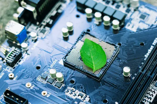
However, sustainable PCB development must be engineering-driven. Material selection should consider electrical performance, thermal stability, mechanical strength, manufacturing compatibility, regulatory requirements, product lifetime, and end-of-life recovery.
For manufacturers and OEMs, the best strategy is often a gradual transition: evaluate sustainable materials, build prototypes, validate reliability, optimize manufacturing processes, and then scale successful solutions into production.
Kingda combines PCB manufacturing, component sourcing, SMT/THT assembly, testing, engineering support, and production traceability in a one-stop manufacturing model, giving customers a practical platform for developing and scaling more environmentally responsible electronic products. (Kingda)