PCB assembly is one of the most important stages in modern electronics manufacturing. It transforms a bare printed circuit board into a functional electronic assembly by accurately mounting and soldering electronic components such as resistors, capacitors, diodes, integrated circuits, connectors, and power devices.
As electronic products become smaller, faster, and more intelligent, the requirements for PCB assembly technology continue to increase. Modern electronics may contain hundreds or thousands of components, fine-pitch packages, high-speed interfaces, RF circuits, power-management systems, and complex mechanical interfaces. Producing these assemblies consistently requires not only advanced equipment but also disciplined process control, engineering expertise, component management, inspection, and testing.
The evolution of PCB assembly manufacturing has transformed the industry from labor-intensive manual soldering into highly automated production environments incorporating SMT placement, reflow soldering, automated optical inspection, X-ray inspection, electrical testing, manufacturing execution systems, and full production traceability.
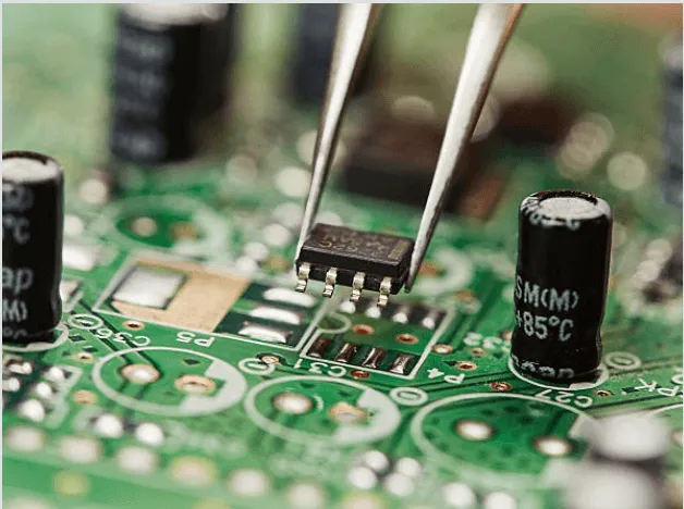
For electronics manufacturers, understanding the core PCB assembly process is essential because assembly quality directly affects electrical performance, reliability, manufacturing yield, product lifespan, and total production cost.
What Is PCB Assembly?
PCB assembly, commonly abbreviated as PCBA, is the process of mounting and soldering electronic components onto a fabricated printed circuit board according to an approved design and manufacturing data package.
A typical PCB assembly process includes:
PCB Preparation → Solder Paste Printing → Component Placement → Reflow Soldering → THT Assembly → Inspection → Electrical Testing → Functional Testing → Final Quality Control
The exact process depends on the product design. Some boards require only SMT assembly, while others combine SMT and through-hole components in a mixed-technology configuration.
The overall objective is to create a reliable electronic assembly that performs according to the original electrical and mechanical requirements.
Evolution of PCB Assembly Technology
Early electronic assemblies relied heavily on manual component insertion and hand soldering. As component density increased, manual processes became increasingly difficult to control.
The development of Surface Mount Technology (SMT) transformed electronic manufacturing by allowing components to be placed directly onto PCB pads.
Modern production lines can integrate:
- Automated solder paste printing
- 3D solder paste inspection
- High-speed pick-and-place machines
- Automated reflow ovens
- Automated optical inspection
- X-ray inspection
- In-circuit testing
- Functional testing
- Automated traceability
- Manufacturing execution systems
These technologies enable manufacturers to produce complex assemblies with higher consistency and lower defect rates.
Today, smart PCB assembly increasingly combines automation, data collection, process monitoring, and digital traceability to improve manufacturing efficiency and quality.
Types of PCB Assembly
Surface Mount Technology Assembly
SMT PCB assembly is currently the dominant assembly technology for many electronic products.
With SMT, components are mounted directly onto copper pads on the surface of a PCB rather than being inserted through drilled holes.
SMT provides several major advantages:
- High component density
- Smaller PCB dimensions
- Automated high-speed production
- Lower material consumption
- Shorter electrical interconnections
- Excellent suitability for high-frequency designs
- Efficient mass production
Modern SMT lines can handle components ranging from standard passive packages to complex packages such as BGA, QFN, CSP, LGA, and other fine-pitch devices.
Kingda’s published SMT capabilities include advanced packages such as BGA, uBGA, QFN, QFP, PoP, CSP, 0201 components, and fine-pitch devices, supported by automated SMT production and inspection equipment.
Through-Hole Technology Assembly
Through-Hole Technology (THT) involves inserting component leads through drilled holes in the PCB and soldering them to pads.
THT remains valuable for components requiring strong mechanical connections, higher current capability, or additional mechanical stability.
Typical THT components include:
- Large connectors
- Transformers
- Relays
- Power components
- Large capacitors
- Terminal blocks
- Switches
THT assembly can use:
- Manual insertion
- Automated insertion
- Wave soldering
- Selective soldering
- Manual soldering
Mixed-Technology Assembly
Many modern electronic products use a combination of SMT and THT assembly.
For example, a power-control PCB may use miniature SMT components for signal processing while using THT connectors, transformers, and high-power components for mechanical and electrical robustness.
This combination provides greater design flexibility while optimizing performance, reliability, and manufacturing cost.
Core PCB Assembly Process
1. Design Data and Engineering Review
Before production begins, the manufacturing team reviews the complete design package.
Typical manufacturing documents include:
- Gerber files
- BOM
- Pick-and-place files
- Assembly drawings
- PCB stack-up
- Fabrication specifications
- Test requirements
- Special process instructions
A complete engineering review helps identify problems before material is purchased or assembly begins.
Typical checks include:
- Component footprint compatibility
- BOM consistency
- Component polarity
- Package orientation
- PCB pad geometry
- Component spacing
- DFM
- DFA
- DFT
- Manufacturing capability
- Component availability
A strong engineering review can significantly reduce production delays and prevent avoidable assembly defects.
2. Solder Paste Printing
For SMT assembly, solder paste is deposited onto PCB pads through a precision stencil.
The solder paste contains metal alloy particles suspended in a flux system.
Printing quality is influenced by:
- Stencil thickness
- Aperture geometry
- Solder paste type
- Paste viscosity
- Squeegee pressure
- Printing speed
- Board support
- Environmental conditions
Poor solder paste deposition can lead to:
- Solder bridges
- Insufficient solder
- Tombstoning
- Open joints
- Voids
For this reason, SPI (Solder Paste Inspection) is often used to verify paste volume, height, area, and position before component placement.
3. Component Placement
Once solder paste has been printed, automated pick-and-place equipment places components onto the PCB.
The machine uses:
- Component feeders
- Nozzles
- Vision systems
- Placement programs
- Fiducial recognition
Vision systems verify component orientation and position to improve placement accuracy.
Modern systems can handle extremely small passive components as well as complex IC packages.
Kingda states that its SMT manufacturing infrastructure includes automated placement equipment, 3D SPI and AOI inspection, and supports advanced component packages for prototype through higher-volume production.
4. First Article Inspection
For new products or production revisions, First Article Inspection (FAI) provides an important verification gate.
Engineers and quality personnel verify:
- Component identity
- Component orientation
- Placement position
- Solder quality
- BOM consistency
- Assembly configuration
The goal is to confirm that the programmed process matches the approved manufacturing documentation before the remaining boards are produced.
5. Reflow Soldering
After component placement, the PCB travels through a controlled reflow oven.
The temperature profile typically contains several stages:
Preheat → Soak → Reflow → Cooling
The profile must be compatible with:
- Solder alloy
- PCB materials
- Component thermal limits
- Board thermal mass
- Package size
- Component distribution
Poor thermal control can produce cold solder joints, solder bridging, component damage, voiding, or warpage.
Modern reflow ovens use multiple heating zones to provide precise temperature control.
6. AOI Inspection
Automated Optical Inspection (AOI) uses cameras and image-processing software to identify visible assembly defects.
AOI can detect:
- Missing components
- Incorrect components
- Misalignment
- Polarity errors
- Solder bridges
- Tombstoning
- Visible solder defects
AOI provides rapid, repeatable inspection across production volumes.
However, AOI cannot see hidden solder connections beneath packages such as BGA devices.
7. X-Ray Inspection
X-ray inspection is used when solder joints cannot be visually inspected.
Typical applications include:
- BGA
- QFN
- LGA
- CSP
- Bottom-terminated components
X-ray inspection can reveal:
- Voids
- Open solder joints
- Bridging
- Insufficient solder
- Misalignment
- Hidden connection defects
For high-reliability products, X-ray inspection provides an additional layer of quality assurance beyond AOI.
8. In-Circuit Testing
ICT (In-Circuit Testing) uses electrical test points and fixtures to verify individual circuit characteristics.
Depending on the design, ICT can identify:
- Open circuits
- Short circuits
- Incorrect component values
- Missing components
- Polarity problems
- Certain soldering defects
ICT is especially valuable for repeat production because dedicated fixtures can provide highly repeatable testing.
9. Functional Testing
Functional testing (FCT) evaluates whether the assembled PCB works as intended in realistic operating conditions.
Depending on the application, functional testing may include:
- Power-up testing
- Voltage verification
- Communication testing
- Sensor testing
- Motor control
- Display operation
- RF communication
- Firmware execution
- Analog and digital signal verification
Functional testing provides a higher-level validation than simple electrical continuity testing.
10. Final Quality Control
After all inspections and tests have been completed, the finished PCB assembly undergoes final quality verification.
The final inspection may include:
- Visual inspection
- Dimensional inspection
- Label verification
- Packaging verification
- Test-record review
- Traceability verification
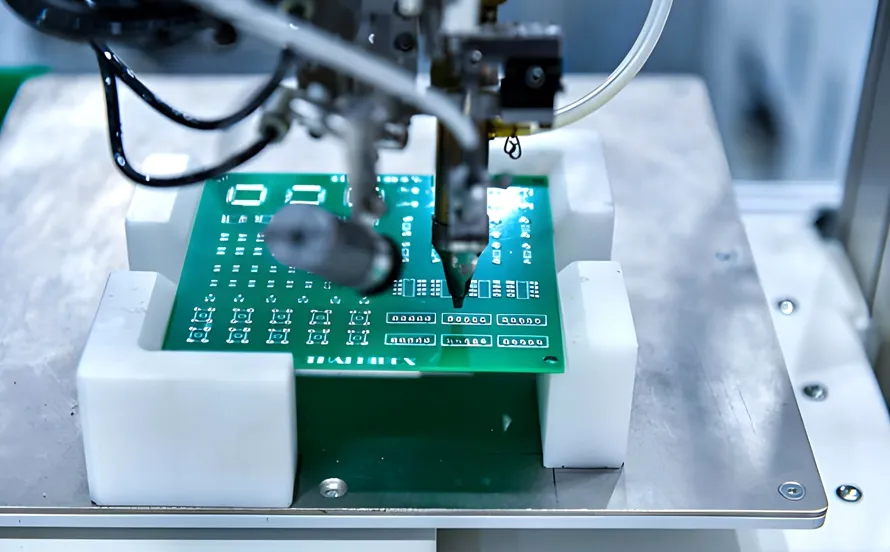
Only boards that meet the defined acceptance criteria should proceed to shipment.
Key Quality Control Technologies in PCB Assembly
A robust PCB assembly quality control system uses multiple inspection stages rather than relying on a single final inspection.
A typical quality flow can be:
IQC → SPI → SMT/THT Assembly → AOI → X-Ray → ICT/FCT → OQC
This layered approach makes it possible to detect defects earlier and prevent problems from moving into subsequent production stages.
Kingda publishes a similar multi-stage quality-control structure, including incoming-material verification, SPI, AOI, X-ray, FAI, ICT, FCT, and final inspection.
Common PCB Assembly Defects and Solutions
Solder Bridging
A solder bridge occurs when solder unintentionally connects adjacent pads.
Common causes include:
- Excessive solder paste
- Incorrect stencil aperture design
- Insufficient pad spacing
- Incorrect component placement
- Poor reflow profile
Solutions include optimizing stencil design, controlling paste volume, improving placement accuracy, and validating the reflow profile.
Cold Solder Joints
A cold solder joint occurs when solder does not properly wet the pad or component termination.
Potential causes include:
- Insufficient reflow temperature
- Insufficient time above liquidus
- Oxidized surfaces
- Improper solder paste storage
- Poor thermal profiling
Reflow profiling and proper solder-paste management are essential for preventing this defect.
Tombstoning
Tombstoning occurs when one end of a small passive component lifts from the PCB during reflow.
Common causes include uneven solder paste deposition or unequal heating on the two pads.
Solutions include:
- Balanced stencil apertures
- Optimized pad geometry
- Improved thermal balance
- Controlled reflow profiles
- Accurate placement
Component Misalignment
Components may become displaced during placement or reflow.
Potential causes include:
- Incorrect pick-and-place coordinates
- Poor fiducial recognition
- Excessive solder paste
- Board movement
- Incorrect component programming
Automated vision systems and first-article inspection help reduce these risks.
Solder Voids
Voids are gas-filled spaces within solder joints.
They are particularly important for power components and thermal pads because excessive voiding can increase thermal resistance.
Stencil design, solder-paste selection, pad geometry, and reflow parameters can all influence void formation.
PCB Assembly Design Considerations
High-quality assembly begins before manufacturing.
Design for Manufacturability
DFM ensures that the PCB can be manufactured within the capabilities of the selected production process.
DFM review may evaluate:
- Trace width
- Clearance
- Pad geometry
- Drill sizes
- Component spacing
- PCB thickness
- Fabrication tolerance
Design for Assembly
DFA focuses specifically on the ease, reliability, and repeatability of assembling components onto the PCB.
Important considerations include:
- Component orientation
- Component spacing
- Assembly sequence
- Fiducial placement
- Stencil access
- THT accessibility
Design for Test
DFT adds test points and other features that make electrical and functional testing easier.
A well-designed DFT strategy can reduce testing time and improve defect detection.
Component Management and Supply Chain Control
PCB assembly quality depends not only on production equipment but also on component quality.
Important component-management practices include:
- Authorized sourcing
- BOM verification
- Manufacturer part-number verification
- Lifecycle monitoring
- Lot traceability
- Moisture-sensitive-device management
- Counterfeit prevention
- Approved alternatives
For long-term products, component obsolescence should also be evaluated before mass production.
A reliable manufacturing partner should be able to identify supply risks before they affect the production schedule.
How to Choose the Right PCB Assembly Manufacturer
Choosing a PCB assembly manufacturer requires more than comparing unit prices.
Manufacturing Capability
Confirm whether the manufacturer supports the technologies required by your design, including:
- SMT
- THT
- Mixed technology
- BGA
- QFN
- CSP
- LGA
- Fine-pitch components
- High-density PCB
- Flexible PCB
- Rigid-flex PCB
Quality System
Look for established quality-management systems and relevant certifications.
Kingda states that it holds ISO 9001, ISO 13485, IATF 16949 and ISO 14001 certifications, along with UL certification and IPC membership.
The applicable certification should always be matched to the product’s industry and regulatory requirements.
Inspection and Testing
A capable manufacturer should provide appropriate access to:
- SPI
- AOI
- X-ray
- FAI
- ICT
- FCT
- Final inspection
The actual inspection plan should reflect the risk and complexity of the project.
Engineering Support
Engineering support is especially valuable during:
- Prototype development
- DFM review
- BOM verification
- Component selection
- Process optimization
- Production transfer
- Design revisions
Kingda provides engineering support covering DFM/DFA, BOM verification, Gerber review, pick-and-place verification, component availability analysis, and manufacturing optimization.
Why Choose Kingda for PCB Assembly?
Kingda is a one-stop PCB and PCBA manufacturing provider founded in 2013 in Shenzhen, China. Its published manufacturing model integrates PCB manufacturing, component procurement, SMT, DIP/THT, finished-product assembly, and testing.
One-Stop Manufacturing
Instead of managing separate suppliers for PCB fabrication, component sourcing, assembly, and testing, customers can coordinate these manufacturing stages through one integrated supplier.
Kingda’s service scope covers:
PCB Design → PCB Fabrication → Component Procurement → SMT/THT Assembly → Testing → Finished Product Assembly
This integrated approach can reduce supplier handoffs and simplify production management.
Prototype to Mass Production
Kingda supports production from prototype and low-volume projects through higher-volume manufacturing, allowing customers to maintain manufacturing continuity as products move through different development stages.
Advanced SMT Capability
Kingda’s published PCBA capabilities support advanced component packages including:
- BGA
- uBGA
- QFN
- QFP
- CSP
- LGA
- PoP
- 0201
- Fine-pitch components
This makes the manufacturing platform suitable for compact and high-density electronic assemblies.
Comprehensive Quality Control
Kingda’s published quality process integrates multiple inspection and testing stages, including SPI, AOI, X-ray, FAI, ICT and FCT. This multi-stage approach helps identify defects before final delivery.
Manufacturing Traceability
Kingda reports using an ERP-based production system capable of supporting product traceability throughout the manufacturing process. This helps connect material, production, quality, and shipment information for stronger process control.
Industry Experience
Kingda states that it serves customers in industries including:
- Medical electronics
- Automotive electronics
- Industrial automation
- Artificial intelligence
- Smart home
- Security
- Electric power
- Communications
These application areas require different combinations of electrical performance, reliability, testing, and production control.
PCB Assembly Best Practices
For reliable long-term results, electronics manufacturers should consider the following principles:
Start Engineering Review Early
Complete DFM, DFA, and DFT analysis before production materials are committed.
Control the Entire Process
Do not treat assembly as only a soldering operation. Component sourcing, material storage, printing, placement, reflow, inspection, testing, and packaging all affect final quality.
Use Multiple Inspection Methods
AOI is effective for visible defects, while X-ray is needed for many hidden solder joints. Electrical and functional tests provide another level of verification.
Maintain Traceability
Record component lots, production batches, inspection results, test results, and revisions so issues can be traced efficiently.
Optimize for Production
A design that works electrically may still be difficult or expensive to manufacture. DFM and DFA should therefore be part of the engineering process rather than an afterthought.
Conclusion
PCB assembly is far more than simply soldering electronic components onto a circuit board. It is an integrated manufacturing discipline that combines engineering, component procurement, SMT and THT technologies, thermal process control, inspection, testing, traceability, and continuous quality improvement.
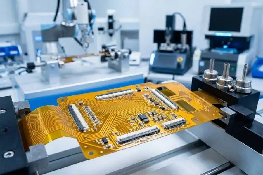
As electronic products become smaller and more complex, the importance of reliable PCB assembly technology will continue to increase.
Manufacturers that combine advanced automation with strong engineering support can improve production consistency, reduce defects, accelerate time-to-market, and support products throughout their entire lifecycle.
Kingda provides an integrated PCB fabrication and PCBA manufacturing solution, covering PCB manufacturing, component sourcing, SMT/THT assembly, inspection, testing, and finished-product integration. Its published capabilities and quality systems support projects ranging from prototypes and low-volume production to larger-scale manufacturing.
For electronics companies seeking a reliable manufacturing partner, the most important criteria are not simply price and capacity. Engineering capability, process control, component quality, inspection depth, traceability, communication, and production scalability all determine whether a PCB assembly project succeeds.