What Is a Semiconductor Test PCB?
A Semiconductor Test PCB is a specialized printed circuit board used to test integrated circuits (ICs), semiconductor devices, and other electronic components during the manufacturing and validation process.
It serves as an electrical interface between the device under test (DUT) and the semiconductor test equipment. The PCB provides controlled electrical connections that allow engineers to measure parameters such as voltage, current, signal integrity, timing, and overall device performance.
Unlike standard circuit boards, semiconductor test boards must meet demanding requirements for electrical accuracy, dimensional precision, reliability, and repeatable performance. Depending on the application, the board may incorporate high-density routing, controlled impedance, fine-pitch connections, specialized materials, and advanced via structures.
For complex semiconductor applications, manufacturers may also combine Semiconductor Test PCB fabrication with advanced technologies such as multilayer construction, HDI, microvias, blind and buried vias, and controlled-impedance structures. GOPCBA provides advanced PCB manufacturing services supporting demanding PCB applications from prototype development to mass production.
Why Are Semiconductor Test PCBs Important?
Semiconductor testing is an essential part of modern electronic manufacturing. Before an IC or semiconductor device is integrated into a final product, it must undergo electrical and functional verification to determine whether it meets its specified performance requirements.
A reliable Semiconductor Test Board helps identify manufacturing defects, electrical abnormalities, connection problems, and performance deviations before defective devices reach customers.
The main benefits include:
- Improved quality control: Detects defective semiconductor devices before final integration.
- Accurate electrical measurement: Provides stable and controlled electrical connections between the DUT and test equipment.
- Higher testing efficiency: Supports automated and repeatable testing processes.
- Improved product reliability: Helps ensure semiconductor devices meet specified performance requirements.
- Reduced manufacturing costs: Early defect detection minimizes rework, recalls, and field failures.
For complex test applications, PCB fabrication quality directly affects measurement accuracy. Proper stack-up design, impedance control, material selection, and manufacturing tolerances are therefore essential.
Types of Semiconductor Test PCBs
Different semiconductor testing stages require different PCB structures and interfaces. Two important types are load boards and probe cards.
Load Board
A load board is primarily used during the final test stage of semiconductor manufacturing. It provides the electrical and mechanical interface between the packaged semiconductor device and the automatic test equipment (ATE).
The load board routes power and high-speed signals between the DUT and the tester while supporting the required mechanical interface.
Typical requirements include:
- High-density routing
- Controlled impedance
- High-frequency signal transmission
- Precise component placement
- High connector reliability
- Effective thermal management
- High mechanical durability
For high-speed semiconductor devices, the load board must maintain signal integrity across the complete electrical path. PCB stack-up, trace geometry, dielectric properties, via structures, and impedance control must therefore be carefully engineered.
Probe Card
A probe card is used primarily for wafer-level semiconductor testing. It establishes electrical contact with individual dies on a semiconductor wafer before the devices are packaged.
Probe cards require extremely precise contact structures because many semiconductor devices contain a large number of closely spaced electrical connections.
Important considerations include:
- Fine-pitch interconnections
- High contact accuracy
- High-density routing
- Low electrical resistance
- Mechanical stability
- Repeatable wafer contact
- Thermal performance
Probe card applications can require advanced PCB technologies and specialized materials depending on the device, test frequency, temperature, and electrical performance requirements.
Semiconductor Test Methods
A IC Test PCB can be used as part of several testing approaches depending on the semiconductor device and production stage.
In-Circuit Testing
In-Circuit Testing (ICT) checks electrical connections and component characteristics using predefined test points.
It can identify issues such as:
- Open circuits
- Short circuits
- Incorrect component values
- Incorrect connections
- Soldering defects
- Electrical abnormalities
ICT is particularly useful for automated production testing because it can rapidly identify manufacturing defects.
Functional Testing
Functional testing evaluates whether the device or assembled circuit performs according to its intended operating requirements.
The test system applies defined inputs and analyzes the resulting outputs to verify the functionality and performance of the device.
For semiconductor-related PCB assemblies, functional testing may include voltage, current, communication, timing, programming, and system-level operation.
GOPCBA also provides PCBA testing services covering electrical and functional testing for assembled circuit boards.
System-Level Testing
System-level testing evaluates the complete electronic system rather than only an individual component.
It can verify whether the semiconductor device performs correctly when integrated with other hardware, software, power-management circuits, communication interfaces, and peripheral components.
This approach provides a more realistic evaluation of overall product performance.
Key Features of Semiconductor Test PCBs
A high-quality Semiconductor Test Board must satisfy demanding electrical, mechanical, and manufacturing requirements.
High Precision
Semiconductor testing often involves very small electrical and mechanical tolerances. The PCB must provide accurate component positioning, stable connections, and consistent electrical characteristics.
Small dimensional deviations can affect contact reliability, impedance, signal transmission, and measurement accuracy.
High-Density Layout
Modern semiconductor devices contain large numbers of pins and increasingly fine-pitch connections.
High-density PCB technologies such as microvias, blind vias, buried vias, fine lines, and HDI structures allow designers to route more connections within a limited board area.
For demanding applications, HDI PCB manufacturing can provide the routing density required by advanced semiconductor test hardware.
Signal Integrity
Signal integrity is critical when testing high-speed semiconductor devices.
Uncontrolled impedance, excessive trace length, crosstalk, reflections, discontinuities, and poor grounding can distort test signals and affect measurement accuracy.
Designers should carefully evaluate:
- Controlled impedance
- Differential-pair routing
- Return paths
- Ground planes
- Trace geometry
- Via transitions
- Crosstalk
- Power integrity
High-speed applications may require specialized laminate materials and carefully engineered PCB stack-ups.
Thermal Management
Semiconductor testing can generate significant heat, particularly when devices operate at high power or under accelerated test conditions.
A properly designed PCB may incorporate:
- Thermal vias
- Copper planes
- Heat sinks
- Thermal interface materials
- High-temperature materials
- Optimized component placement
Effective thermal management helps maintain stable operating conditions and prevents excessive temperature from affecting test accuracy or damaging components.
Durability and Repeatability
Test boards may be used for thousands or even millions of test cycles. Mechanical wear, thermal cycling, repeated connector insertion, and electrical stress can gradually affect PCB performance.
A durable test PCB should therefore use appropriate materials, reliable surface finishes, robust solder joints, and suitable mechanical structures.
Semiconductor Test PCB Design Considerations
Designing a Semiconductor Test PCB requires close coordination between electrical design, mechanical engineering, thermal management, and PCB manufacturing.
HDI and High-Density Interconnect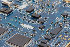
HDI technology can significantly increase routing density by using fine lines, microvias, blind vias, buried vias, and sequential lamination.
Before designing an HDI test board, engineers should confirm the manufacturer’s capabilities for:
- Minimum line and space
- Minimum microvia diameter
- Capture pad size
- Microvia aspect ratio
- Stacked or staggered microvias
- Copper filling
- Layer registration
- Sequential lamination
Designing according to validated manufacturing limits helps improve yield and reduce production risks.
Controlled Impedance
Controlled impedance is essential for high-speed test signals.
The target impedance should be established during the stack-up design process. Engineers need to consider dielectric thickness, copper thickness, trace width, trace spacing, material properties, and reference-plane configuration.
The final PCB should be manufactured according to the approved impedance specification and verified using appropriate test methods.
For high-speed applications, high-speed PCB manufacturing can help address stack-up, material selection, impedance control, and signal-integrity requirements.
Material Selection
PCB materials directly influence electrical performance, thermal stability, mechanical reliability, and manufacturing cost.
Depending on the application, semiconductor test boards may use:
- Standard FR-4
- High-Tg materials
- Low-loss materials
- High-frequency laminates
- High-speed materials
- Specialized multilayer constructions
Material selection should consider operating frequency, temperature, signal speed, dielectric properties, thermal requirements, and expected production volume.
Mechanical Accuracy
Mechanical dimensions are particularly important for test boards that interface with semiconductor packages, sockets, connectors, probes, and automated test equipment.
Critical mechanical requirements may include:
- Board thickness
- Hole position
- Connector position
- Component clearance
- Board outline
- Mounting-hole accuracy
- Flatness
- Warpage control
Accurate mechanical design ensures reliable contact between the test PCB and the DUT or test equipment.
Semiconductor Test PCB Manufacturing Process
A typical IC Test PCB manufacturing process includes several stages.
1. Design and Engineering Review
The PCB design, stack-up, materials, impedance requirements, mechanical dimensions, and manufacturing specifications are reviewed before production.
2. DFM Analysis
Design for Manufacturing (DFM) analysis identifies potential production problems such as insufficient spacing, unsupported via structures, registration risks, and manufacturing limitations.
Early DFM review can reduce redesigns and improve production yield.
3. PCB Fabrication
The PCB is manufactured according to the approved design and process specifications.
Depending on the design, manufacturing may include:
- Multilayer lamination
- Laser drilling
- Mechanical drilling
- Copper plating
- Pattern plating
- Etching
- Solder mask
- Surface finishing
- Electrical testing
GOPCBA supports PCB production from prototypes through volume manufacturing, including multilayer, HDI, high-speed, high-frequency, rigid-flex, heavy-copper, and other advanced PCB technologies.
4. Inspection and Testing
Manufactured boards are inspected to verify dimensions, electrical continuity, surface quality, solder-mask condition, and other customer-defined requirements.
For assembled test boards, additional inspection and testing may include AOI, X-ray, ICT, and functional testing.
5. Assembly and Final Integration
If components are required, the PCB can proceed to SMT, through-hole assembly, inspection, programming, and functional testing.
GOPCBA provides PCB assembly services covering rigid, flexible, rigid-flex, multilayer, HDI, high-TG, high-frequency, heavy-copper, metal-core, and controlled-impedance PCB assemblies.
How to Choose a Semiconductor Test PCB Manufacturer
Selecting the right manufacturer is critical because test boards often have tighter electrical and mechanical requirements than standard PCBs.
Consider the following factors:
Manufacturing Capability
Verify that the manufacturer can support the required layer count, HDI structures, microvias, fine lines, controlled impedance, high-frequency materials, and specialized PCB construction.
Engineering Support
A capable supplier should provide DFM review, stack-up analysis, material recommendations, Gerber verification, and manufacturing feasibility analysis.
Testing Capability
The manufacturer should have appropriate inspection and testing equipment to verify PCB quality and assembled-board functionality.
GOPCBA’s published PCBA capabilities include AOI, X-ray, ICT, functional testing, programming, first article inspection, and additional reliability testing.
Prototype-to-Mass-Production Support
It is beneficial to work with a manufacturer that can support the complete product lifecycle:
Prototype → Engineering Validation → Low-Volume Production → Mass Production
This reduces the risk of process changes when a validated test board moves into production.
One-Stop PCB and PCBA Services
A manufacturer capable of both PCB fabrication and assembly can simplify project management and reduce communication between multiple suppliers.
GOPCBA provides integrated PCB manufacturing, component procurement, SMT/THT assembly, testing, and other electronic manufacturing services, allowing customers to manage complex PCB projects through one manufacturing partner.
Conclusion
A Semiconductor Test PCB is a critical component in semiconductor testing, providing the electrical and mechanical interface between the device under test and test equipment.
As semiconductor devices become smaller, faster, and more complex, test boards require increasingly advanced technologies, including HDI, microvias, controlled impedance, high-speed materials, high-density routing, and advanced thermal management.
The right Semiconductor Test Board must combine electrical performance, mechanical precision, manufacturing reliability, and long-term repeatability.
By selecting an experienced PCB manufacturer with strong engineering capabilities, advanced fabrication technology, comprehensive testing resources, and prototype-to-production support, semiconductor companies can improve test accuracy, reduce manufacturing risks, and achieve more reliable production results.