SMT Flying Probe Testing: Process, Capabilities, Limitations, and Benefits
What Is SMT Flying Probe Testing?
SMT Flying Probe Testing is an electrical testing method used during surface mount technology (SMT) production to verify PCB assembly quality, component connections, and circuit integrity.
Unlike traditional ICT systems that use a fixed bed-of-nails fixture, a flying probe tester uses movable probes to access designated test points on the PCB. The probes travel along the X-Y axes according to programmed coordinates and contact individual test points to perform electrical measurements and circuit verification.
This fixtureless approach makes Flying Probe Test particularly suitable for prototypes, low-volume production, and products that change frequently because dedicated test fixtures are generally not required. It can also be integrated into a broader PCB Assembly Testing strategy to improve manufacturing quality and reduce the risk of defective boards reaching subsequent production stages.
SMT Flying Probe Testing Specifications
The applicable testing range depends on the equipment configuration and PCB design. Typical specifications for the referenced SMT flying probe process include:
| Parameter | Testing Capability |
|---|---|
| Maximum PCBA size | 500 × 410 mm |
| Minimum PCBA size | 50 × 50 mm |
| PCBA thickness | 0.6–6 mm |
| Maximum component height | 60 mm |
| Minimum passive package | 0201 |
| Resistor measurement range | 1 Ω–1 GΩ |
| Capacitor measurement range | 10 pF–1 F |
| Inductor measurement range | 10 μH–1 H |
Actual capabilities should be confirmed according to the PCB dimensions, component distribution, test-point accessibility, and specific equipment configuration before production.
For projects requiring a complete manufacturing solution, SMT Assembly can be combined with PCB fabrication, component sourcing, inspection, and electrical testing through an integrated PCBA production process.
What Components Can Be Tested by Flying Probe?
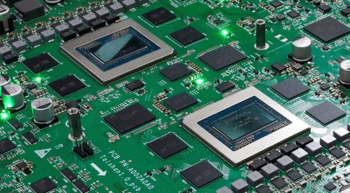
A flying probe system can perform a wide range of electrical measurements and connection checks. However, its effectiveness depends on whether the component can be electrically accessed and whether the tester can reproduce the conditions required for the intended test.
Passive Components
Resistors, capacitors, inductors, and similar passive components can generally be tested for electrical values, continuity, open circuits, and short circuits.
These tests can help identify common SMT manufacturing defects, including:
- Solder bridges
- Open solder joints
- Missing components
- Incorrect component placement
- Incorrect component values
- Poor electrical connections
For passive components, the flying probe system can measure resistance, capacitance, and inductance within the applicable equipment range.
LEDs, Diodes, Transistors, and MOSFETs
Flying probe testing can verify basic electrical characteristics of LEDs, diodes, transistors, and MOSFETs.
For example, diode and LED testing may include forward-voltage measurements, while transistor and MOSFET tests can verify basic conduction characteristics. These measurements help identify incorrect polarity, defective components, and soldering-related problems.
Analog ICs
Certain analog ICs can be checked for pin connectivity, shorts, opens, and other basic electrical conditions.
Ground-referenced diode testing can also help verify IC pin conditions and solder connections. This can reveal problems such as open solder joints, incorrect component orientation, or abnormal connections.
However, flying probe testing should not be considered a replacement for complete functional testing when an IC requires complex operating conditions or dynamic signals.
LDOs, Relays, and Optocouplers
Some power and signal-control components can be evaluated by applying appropriate electrical stimuli and measuring their responses.
For example, an LDO may be checked by applying an input voltage and measuring its output voltage. Relays and optocouplers may be evaluated for basic input-output behavior when the required test conditions can be safely reproduced.
Filters, Fuses, Switches, Connectors, and TVS Devices
Flying probes can also verify continuity and electrical connections for filters, fuses, switches, connectors, and TVS devices.
For example, a fuse can be checked for continuity, while connectors and switches can be tested for shorts or unintended connections. These tests are useful for detecting solder bridges and other assembly defects.
For projects requiring broader inspection coverage, PCBA Testing can combine electrical testing with visual inspection, AOI, X-ray inspection, ICT, or functional testing according to the product’s requirements.
Components and Devices That Are Difficult to Test
Flying probe testing is highly flexible, but it is not suitable for every component or every type of functional verification.
BGA Components
BGA solder joints are located underneath the package, making direct probe access to individual solder balls impractical.
For BGA assemblies, X-ray inspection is generally more appropriate for evaluating hidden solder joints. A comprehensive manufacturing process can combine flying probe or electrical testing with X-ray inspection where required.
Complex Digital ICs
Complex digital ICs may contain large numbers of pins and sophisticated internal logic. Their complete operation often requires high-speed signals, specific timing conditions, power sequencing, communication protocols, and other dynamic test conditions.
Therefore, flying probe testing is generally better suited to verifying connectivity and basic electrical characteristics rather than performing comprehensive functional validation of complex digital ICs.
Thyristors
Thyristors require specific triggering conditions to switch between operating states. A standard flying probe system may not be able to reproduce the required gate-triggering and operating conditions accurately enough for complete functional verification.
Operational Amplifiers and Comparators
Operational amplifiers and comparators normally require defined supply voltages, input signals, feedback networks, and operating conditions.
Because a flying probe system primarily performs programmed electrical measurements, it may not provide the complete dynamic environment required for functional verification of these devices.
Solid-State Relays
Solid-state relays may require specific voltage, current, and load conditions to verify their switching behavior. If the flying probe system cannot reproduce the actual operating environment, a complete load test cannot be performed accurately.
Large or Irregular Components
Large or irregularly shaped components can make test-point access difficult. Physical obstruction, limited probe clearance, or inaccessible test points may prevent complete coverage.
Specialized Sensors and RF or MEMS Devices
Some components require specialized external stimuli or environmental conditions. Examples include:
- Infrared devices
- Photoresistors
- Varistors
- Hall-effect sensors
- Other sensors
- RF components
- Acoustic components
- MEMS devices
For these products, dedicated functional or application-specific testing may be necessary because a conventional flying probe system cannot reproduce all required operating conditions.
What Manufacturing Risks Can Flying Probe Testing Reduce?
The primary purpose of PCB Assembly Testing is to identify manufacturing and electrical defects as early as possible.
Detecting SMT Manufacturing Defects
Flying probe testing can help identify:
- Open circuits
- Short circuits
- Solder bridges
- Missing components
- Incorrect component orientation
- Incorrect component values
- Poor solder connections
- Certain defective components
Early detection prevents defective assemblies from moving further through the manufacturing process.
Identifying Design-Related Problems
Electrical testing can also expose problems associated with PCB design or circuit connectivity.
When unexpected electrical relationships are detected, engineering teams can investigate PCB layout, component connections, test-point design, and other potential causes. This feedback can help improve future revisions.
Controlling Component-Related Problems
Electrical measurements can identify abnormal component values or behavior and help distinguish assembly defects from component-related issues.
Combined with incoming material inspection and component traceability, electrical testing contributes to a more comprehensive quality-control system. GOPCBA’s quality process includes incoming inspection, production control, PCBA testing, and final quality checks.
When Should Flying Probe Testing Be Performed?
A practical SMT production sequence is:
SMT Assembly → AOI Inspection → Flying Probe Testing → Through-Hole Assembly / Further Processing
Performing flying probe testing after SMT and AOI but before subsequent through-hole or manual assembly can provide several advantages.
Early Defect Detection
Testing immediately after SMT helps identify electrical and assembly defects before the PCB enters later production stages.
If a defect is found after additional components have been installed, troubleshooting and repair can become more complicated.
Easier Troubleshooting
Testing the SMT stage before additional assembly reduces the number of variables involved in troubleshooting.
This can make it easier for engineers to determine whether the problem originated from component placement, soldering, PCB fabrication, or another manufacturing stage.
Lower Rework Costs
Identifying defects before through-hole assembly or final integration can reduce unnecessary disassembly and rework.
This is particularly important for prototype and low-volume projects where engineering changes and repeated production runs are common. GOPCBA provides prototype, low-volume, and high-volume assembly services with integrated inspection and testing capabilities.
Flying Probe Testing vs. Other PCBA Testing Methods
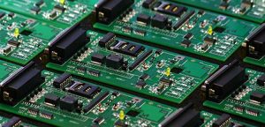
Flying probe testing should be selected according to the product’s testing objectives rather than treated as a universal replacement for other inspection methods.
| Testing Method | Primary Purpose | Typical Application |
|---|---|---|
| Flying Probe Test | Electrical connectivity and component measurements | Prototypes and low-volume production |
| AOI | Visual inspection of component placement and soldering | SMT production |
| X-Ray | Hidden solder-joint inspection | BGA, QFN and other concealed joints |
| ICT | Electrical testing using a dedicated fixture | Repetitive production |
| Functional Test | Verifies actual product operation | Final product validation |
A robust production strategy may use multiple inspection and testing methods. GOPCBA’s published quality-control flow includes IQC, SPI, SMT/THT assembly, AOI, X-ray, ICT/FCT, and OQC, depending on project requirements.
How to Choose the Right Testing Method for Your PCBA
The appropriate testing strategy depends on several factors:
PCB Design
Consider board size, component density, test-point accessibility, component package types, and circuit complexity.
Production Volume
Flying probe testing is particularly attractive when production volumes are low or designs change frequently because it avoids much of the dedicated-fixture investment associated with traditional fixture-based testing.
For high-volume products with stable designs, fixture-based ICT or other automated testing methods may become more economical.
Product Function
If the goal is to identify opens, shorts, incorrect component values, and basic electrical problems, flying probe testing can provide useful coverage.
If the product requires communication verification, high-speed signal validation, sensor stimulation, RF testing, or complete system-level validation, additional functional testing may be required.
Required Quality Level
Medical, automotive, industrial, aerospace, and other mission-critical products may require multiple inspection and testing stages rather than relying on a single testing method.
A qualified PCBA Testing strategy should therefore be developed according to the product’s electrical characteristics, application environment, production volume, and quality requirements.
Why Choose GOPCBA for SMT and PCBA Testing?
GOPCBA provides integrated PCB manufacturing and assembly services covering PCB fabrication, component procurement, SMT assembly, through-hole assembly, inspection, electrical testing, and final product integration.
For customers developing new electronic products, Rapid PCBA Prototyping can support prototype and small-batch requirements with SMT and through-hole assembly, AOI and X-ray inspection, and functional testing options.
For production projects, Turnkey PCB Assembly integrates component procurement, PCB assembly, inspection, testing, and subsequent manufacturing processes into a coordinated supply chain.
Customers requiring specialized manufacturing can also consider Mixed Technology PCB Assembly when a product combines SMT and through-hole components.
For industrial applications, Industrial PCB Assembly supports production projects that require assembly, inspection, testing, and final integration.
Conclusion
SMT Flying Probe Testing is a flexible electrical testing method for identifying opens, shorts, incorrect component values, connection problems, and other manufacturing defects after SMT assembly.
Its fixtureless architecture makes it especially useful for prototypes, engineering builds, low-volume production, and products with frequent design changes. However, it cannot replace every form of inspection or functional testing. BGA solder joints, complex digital ICs, RF devices, sensors, and other specialized components may require X-ray inspection or dedicated functional test systems.
For the best results, flying probe testing should be integrated into a broader PCB Assembly Testing strategy that combines AOI, X-ray, ICT, functional testing, and final inspection according to the specific requirements of the PCBA. A properly planned testing process can identify defects earlier, reduce rework costs, improve manufacturing consistency, and increase overall product reliability.
To discuss your PCB assembly and testing requirements, visit GOPCBA and submit your Gerber files, BOM, and testing requirements for engineering evaluation.