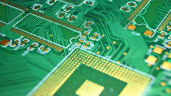
In modern PCB manufacturing, PCB Surface Finish is an essential process for protecting exposed copper, maintaining good solderability, and ensuring reliable electrical performance. Bare copper can react with oxygen, moisture, and other environmental contaminants, resulting in oxidation and surface deterioration over time. If the copper surface is not properly protected, oxidation may negatively affect soldering quality, electrical connectivity, and the long-term reliability of the finished PCB.
For this reason, selecting the appropriate PCB Surface Treatment is an important part of the overall PCB manufacturing process. Different surface finishes provide different levels of solderability, surface flatness, corrosion resistance, mechanical durability, storage stability, and cost efficiency.
As an experienced PCB manufacturer, Kingda works with a variety of surface finishing technologies to meet different PCB design and assembly requirements. The most suitable finish depends on factors such as component pitch, PCB structure, assembly technology, operating environment, electrical requirements, and production budget.
The following sections introduce eight commonly used PCB Surface Finish technologies and explain their main characteristics, advantages, limitations, and typical applications.
1. Hot Air Solder Leveling (HASL)
Hot Air Solder Leveling (HASL) is one of the traditional and widely used PCB Surface Treatment processes. It is commonly known as solder spraying or tin spraying.
During the HASL process, the exposed copper surface of the PCB is coated with molten solder. Heated compressed air is then used to remove excess solder and level the coating, forming a protective solder layer over the copper surface.
The primary purpose of HASL is to protect the copper from oxidation while providing a solderable surface for component assembly. During the process, copper and solder interact at the interface and form a copper-tin intermetallic compound.
The PCB is immersed in molten solder, and air knives remove excess solder before the solder solidifies. Proper control of solder temperature, air pressure, conveyor speed, and other process parameters helps improve coating consistency and reduce solder bridging.
The main advantages of HASL include:
- Good solderability
- Relatively low manufacturing cost
- Mature and widely established process
- Suitable for many conventional PCB applications
However, HASL generally provides less uniform surface flatness than newer surface finishes. Therefore, it may not be the preferred option for extremely fine-pitch components, micro-BGA packages, or highly dense PCB assemblies.
For standard PCB applications where cost efficiency and reliable solderability are the main priorities, HASL remains a practical option.
2. Organic Solderability Preservative (OSP)
Organic Solderability Preservative (OSP) is a chemical PCB Surface Treatment primarily used to protect exposed copper surfaces from oxidation while maintaining good solderability.
During the OSP process, a thin organic protective film is chemically formed on the cleaned copper surface. This film acts as a temporary barrier against oxidation, moisture, and environmental contamination during storage and handling.
During soldering, the protective organic layer is removed by the flux and soldering heat, exposing the clean copper surface so that it can form a reliable solder joint.
One of the most important advantages of OSP is its excellent surface flatness. Since the coating is extremely thin, it does not significantly change the geometry of the copper pads. This makes OSP particularly suitable for fine-pitch components and high-density PCB assemblies.
Key advantages of OSP include:
- Excellent surface flatness
- Good solderability
- Relatively low cost
- Suitable for fine-pitch PCB assembly
- Low material consumption
- Compatible with appropriate lead-free manufacturing processes
However, OSP generally has a more limited storage life than some metallic finishes. Proper packaging, storage temperature, humidity control, and handling are therefore important to maintain surface quality before assembly.
3. Electroplated Nickel and Gold
Electroplated nickel and gold is a PCB Surface Finish used in applications requiring good electrical performance, corrosion resistance, and mechanical durability.
The process generally involves depositing a nickel layer onto the copper surface, followed by an electroplated gold layer. The nickel layer acts as a barrier between copper and gold, helping reduce copper diffusion while improving mechanical stability and corrosion resistance.
Electroplated gold can generally be classified into soft gold and hard gold.
Soft gold has a relatively high-purity gold surface and is commonly used for applications such as wire bonding and semiconductor packaging.
Hard gold contains alloying elements that increase hardness and wear resistance. It is therefore suitable for contact fingers, connectors, switches, and other areas exposed to repeated mechanical contact.
Compared with conventional solderable finishes, electroplated nickel and gold can provide better durability and electrical contact performance. However, the process is generally more expensive and may not be necessary for ordinary soldering surfaces.
4. Electroless Nickel Immersion Gold (ENIG)
Electroless Nickel Immersion Gold (ENIG) is one of the most widely used modern PCB Surface Finish technologies, particularly for high-density and high-reliability PCB applications.
ENIG consists of an electroless nickel layer covered by a thin immersion gold layer. The nickel layer provides a stable and durable foundation, while the immersion gold layer protects the underlying nickel surface and maintains good solderability.
A major advantage of ENIG is its excellent surface flatness. This makes it well suited for fine-pitch components, BGA packages, and other high-density PCB assemblies.
Additional advantages include:
- Excellent surface flatness
- Good solderability
- Good corrosion resistance
- Stable electrical performance
- Relatively good storage stability
- Suitable for high-density PCB assembly
Because of these characteristics, ENIG is frequently selected when PCB designers need a balance between surface quality, reliability, assembly performance, and cost.
However, ENIG requires tighter process control than simpler surface finishes. The quality of the nickel layer, immersion gold layer, and overall chemical process can directly affect PCB reliability.
5. Immersion Tin
Immersion Tin is a chemical surface treatment in which a thin layer of tin is deposited directly onto the exposed copper surface.
One of the main benefits of immersion tin is its relatively flat surface. Unlike HASL, the process does not require molten solder to be leveled using air knives, which helps reduce surface unevenness.
The resulting surface provides good solderability and is compatible with many common lead-free soldering processes.
The main advantages of Immersion Tin include:
- Good surface flatness
- Good solderability
- Suitable for fine-pitch components
- Compatible with lead-free soldering
- Relatively uniform surface coating
However, immersion tin requires appropriate storage and handling conditions. Excessive storage time, high humidity, contamination, or improper packaging may affect the surface condition and solderability.
Therefore, production scheduling and storage management should be considered when selecting immersion tin.
6. Immersion Silver
Immersion Silver is another chemical PCB Surface Treatment that provides a relatively flat and solderable surface.
During the process, a thin silver layer is deposited onto the exposed copper surface. The resulting finish provides good solderability and excellent surface flatness, making it suitable for fine-pitch PCB assembly.
Compared with some other metallic finishes, immersion silver also has a relatively simple process structure.
Its advantages include:
- Excellent surface flatness
- Good solderability
- Suitable for fine-pitch assembly
- Good compatibility with lead-free soldering
- Suitable for selected high-density PCB applications
However, silver surfaces can be affected by certain environmental conditions and may gradually lose their original appearance or become tarnished.
Compared with ENIG, immersion silver generally has lower mechanical wear resistance because it does not include a nickel barrier layer beneath the silver.
Therefore, the application environment and mechanical requirements should be carefully evaluated before selecting Immersion Silver.
7. Electroless Nickel Electroless Palladium Immersion Gold (ENEPIG)
Electroless Nickel Electroless Palladium Immersion Gold (ENEPIG) is a high-performance PCB Surface Finish designed for applications requiring excellent electrical performance, solderability, corrosion resistance, and long-term reliability.
Compared with ENIG, ENEPIG introduces an additional palladium layer between the nickel and gold layers.
The basic structure can be described as:
Copper → Nickel → Palladium → Gold
The palladium layer acts as an additional barrier and helps improve corrosion resistance and surface stability. The thin immersion gold layer protects the palladium and provides a suitable surface for soldering and electrical connections.
ENEPIG is particularly suitable for:
- High-reliability electronic products
- Semiconductor packaging
- Wire bonding
- Fine-pitch components
- Advanced PCB assemblies
- Applications requiring multiple interconnection technologies
One of the main advantages of ENEPIG is its versatility. It can support soldering, wire bonding, and electrical contact requirements within the same PCB design.
The main limitation is cost. The additional palladium layer and more complex chemical process generally make ENEPIG more expensive than conventional finishes such as HASL or OSP.
8. Hard Gold Plating
Hard Gold Plating is primarily used in PCB areas that must withstand repeated mechanical contact, friction, insertion, and removal.
Unlike solderable surface finishes that are normally applied to component pads, hard gold is typically applied selectively to specific contact areas.
Typical applications include:
- Gold fingers
- Edge connectors
- Switch contacts
- Connector contacts
- Repeated insertion and removal interfaces
The high hardness and wear resistance of hard gold help extend the service life of contact surfaces while maintaining reliable electrical connections.
The required gold thickness and plating conditions should be determined according to the expected number of mating cycles, mechanical stress, electrical requirements, and operating environment.
For this reason, Hard Gold Plating is generally not necessary across the entire PCB. Selective application can provide the required performance while helping control manufacturing costs.
How to Choose the Right PCB Surface Finish?
Choosing the appropriate PCB Surface Treatment requires consideration of multiple factors rather than simply selecting the lowest-cost option.
Important factors include:
- Soldering requirements – Different assembly processes may require different surface characteristics.
- Component density – Fine-pitch and BGA components generally benefit from highly flat surfaces.
- Electrical performance – Certain applications require stable and reliable contact characteristics.
- Mechanical durability – Connector and contact areas may require hard gold or other wear-resistant finishes.
- Storage requirements – The expected storage period and environmental conditions can influence finish selection.
- Operating environment – Temperature, humidity, corrosion, and contamination should be considered.
- Production volume – High-volume production may require a balance between process stability and manufacturing cost.
- Overall budget – More advanced surface finishes generally involve higher material and processing costs.
For standard PCB applications where cost efficiency and good solderability are the primary requirements, HASL can be an economical solution.
For fine-pitch and high-density PCB assemblies, OSP, ENIG, or Immersion Silver may provide better surface flatness.
For high-reliability applications requiring excellent surface stability, wire bonding, or multiple interconnection methods, ENIG or ENEPIG may be more appropriate.
For connector areas exposed to repeated mechanical contact, Hard Gold Plating can provide the necessary wear resistance.
At Kingda, surface finish selection can be evaluated together with the PCB structure, component package, assembly process, operating environment, reliability requirements, and production volume to achieve an appropriate balance between performance and cost.
Conclusion
There is no single PCB Surface Finish that is ideal for every application. Each PCB Surface Treatment technology has its own advantages, limitations, manufacturing requirements, and suitable application scenarios.
HASL provides good solderability and cost efficiency, while OSP offers excellent flatness and effective copper protection. ENIG provides a strong combination of flatness, solderability, corrosion resistance, and reliability. Immersion Tin and Immersion Silver are also suitable options for specific PCB assembly requirements.
For more demanding applications, ENEPIG provides excellent performance for advanced interconnection and high-reliability applications, while Hard Gold Plating is particularly suitable for areas requiring repeated electrical contact and high wear resistance.
Therefore, PCB surface treatment should be selected according to the actual requirements of the final product. By evaluating solderability, surface flatness, electrical performance, mechanical durability, storage conditions, operating environment, production volume, and cost together, manufacturers can achieve a better balance between PCB reliability and manufacturing efficiency.
Kingda can provide professional recommendations based on the PCB structure, application requirements, assembly process, and expected production conditions, helping customers select a suitable surface finish for their specific PCB applications.