Power Integrity Solutions for High-Layer-Count PCBs in Satellite Communication
Satellite communication electronics operate under demanding electrical, thermal, mechanical, and environmental conditions. In these systems, the stability of power delivery directly affects communication reliability, signal quality, electromagnetic compatibility, and long-term system performance.
As satellite payloads integrate more RF channels, high-speed processors, communication interfaces, and power-management circuits, conventional PCB structures may no longer provide sufficient routing density or electrical performance. A carefully engineered High-Layer-Count PCB can provide additional routing capacity, dedicated power and ground planes, controlled impedance structures, and improved power distribution.
For demanding aerospace and satellite applications, PCB manufacturing must combine material selection, stack-up engineering, precision lamination, copper processing, impedance control, and rigorous inspection. GOPCBA provides advanced PCB manufacturing solutions covering multilayer, HDI, high-frequency, high-speed, controlled-impedance, heavy-copper, and other specialized PCB technologies.
1. High-Performance Materials for Stable Power Delivery
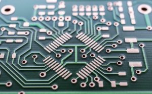
Material selection is one of the first factors affecting the electrical performance of a satellite communication PCB.
A Satellite Communication PCB may need to support RF circuits, high-speed digital interfaces, power distribution, and sensitive analog circuits on the same board. Different functional areas can therefore have significantly different electrical requirements.
Low-loss and high-performance laminates can help reduce transmission loss in high-frequency circuits, while high-Tg materials can provide improved thermal stability for demanding applications. Depending on the operating frequency and electrical specifications, materials such as high-frequency laminates, Rogers materials, PTFE-based materials, and other specialized dielectric systems may be considered.
For RF and microwave applications, dielectric constant, dissipation factor, copper surface characteristics, dielectric thickness, and layer registration all influence electrical performance. Proper material selection should therefore be based on the complete electrical and mechanical requirements rather than simply choosing the lowest-cost laminate.
A stable material supply and consistent material properties are equally important. Variations in dielectric thickness or dielectric properties can affect impedance, signal propagation, and power distribution characteristics.
2. Multilayer Stack-Up and Power-Ground Plane Optimization
A carefully designed stack-up is central to Power Integrity PCB performance.
High-layer-count construction allows designers to dedicate specific layers to power, ground, high-speed signals, RF routing, and other functional circuits. Power and ground planes can be positioned close together to reduce loop inductance and provide a more stable return-current path.
A well-engineered stack-up can provide:
- Dedicated power distribution layers
- Continuous ground reference planes
- Controlled dielectric thickness
- Shorter high-frequency return paths
- Improved isolation between functional circuits
- Better signal and power integrity
- Greater routing density
For complex satellite communication electronics, different voltage domains may also require careful partitioning. Power domains should be organized to reduce unwanted coupling between sensitive analog, RF, digital, and high-current circuits.
GOPCBA supports advanced Multilayer PCB Manufacturing, including high-layer-count structures and complex multilayer fabrication requirements. Its published capabilities include multilayer PCB, high-frequency PCB, controlled-impedance PCB, HDI PCB, and other advanced technologies.
3. Heavy Copper for High-Current Power Distribution
Power distribution networks in satellite electronics may include areas with relatively high current density. In these regions, conventional copper thickness may not provide sufficient current-carrying capability or thermal performance.
Heavy-copper PCB technology can increase current-carrying capacity while reducing conductor resistance and voltage drop.
The design of high-current power regions should consider:
- Copper thickness
- Trace width
- Power-plane area
- Current density
- Via current capacity
- Thermal distribution
- Voltage drop
- Local temperature rise
Increasing copper thickness alone does not automatically solve power-integrity problems. Copper distribution must also be optimized so that current does not become concentrated in localized regions.
For multilayer designs, power planes and vias should be coordinated to create efficient current paths between layers. Where necessary, multiple vias can be used to distribute current and improve thermal transfer.
Heavy-copper PCB manufacturing is particularly useful for power electronics and high-current applications, but the fabrication process requires careful control of etching, plating, copper distribution, and dimensional compensation.
4. Fine-Line Routing and Controlled Impedance
Satellite communication systems frequently combine RF, high-speed digital, and power circuits. Maintaining stable electrical characteristics across these different circuits is therefore essential.
High-Frequency PCB structures require accurate control of trace geometry, dielectric thickness, copper characteristics, and reference-plane configuration.
Controlled impedance should be established during the stack-up design stage rather than treated as a final inspection item. Key parameters include:
- Trace width
- Trace thickness
- Dielectric thickness
- Dielectric constant
- Copper surface profile
- Reference-plane spacing
- Differential-pair geometry
- Target impedance tolerance
For high-speed and RF circuits, uncontrolled manufacturing variations can change impedance and increase signal loss or reflections.
GOPCBA provides high-frequency and controlled-impedance PCB manufacturing capabilities for demanding RF, microwave, communication, and high-speed applications.
5. Mixed-Material Lamination for RF and Digital Integration
Satellite communication equipment may require multiple PCB material characteristics within the same electronic platform.
RF circuits can require low-loss dielectric materials, while digital and power sections may use different material systems. Mixed-material construction can therefore provide a practical solution when properly engineered.
However, combining different materials introduces additional manufacturing considerations, including:
- Different thermal expansion characteristics
- Resin compatibility
- Lamination temperature
- Lamination pressure
- Dielectric thickness
- Layer registration
- Interlayer bonding
- Mechanical reliability
The lamination process must be carefully controlled to maintain dimensional stability and reliable interconnection between different material systems.
Mixed-material PCB construction can be especially valuable for communication systems that combine RF, high-speed digital, and power functions. The stack-up should be validated during engineering review before production begins.
6. Power Integrity and Electromagnetic Noise Control
Power integrity and electromagnetic compatibility are closely connected.
Rapid changes in current can produce voltage fluctuations, ground bounce, and electromagnetic noise. If the power distribution network is not properly designed, these disturbances can couple into sensitive RF or high-speed signal circuits.
A robust Power Integrity PCB design should therefore consider:
- Continuous reference planes
- Short return-current paths
- Power-plane segmentation
- Grounding strategy
- Decoupling capacitor placement
- Via configuration
- High-current path optimization
- Separation of sensitive and noisy circuits
Ground planes should remain as continuous as practical, particularly beneath high-speed and RF signal paths. Unnecessary plane discontinuities can force return currents to take longer paths, increasing loop area and electromagnetic radiation.
For high-frequency circuits, controlled impedance, appropriate reference planes, differential routing, and EMI/EMC considerations should be addressed together during PCB design. GOPCBA’s PCB design services support stack-up design, impedance calculation, multilayer design, high-frequency design, HDI, blind/buried vias, and EMC considerations.
7. Precision Manufacturing and Quality Control
The performance of a high-layer-count satellite PCB depends not only on the design but also on manufacturing consistency.
As the number of layers increases, registration accuracy, lamination control, drilling, copper plating, etching, and electrical testing become increasingly important.
A complete manufacturing quality system should monitor critical parameters throughout the production process, including:
- Inner-layer registration
- Lamination thickness
- Copper thickness
- Hole quality
- Via reliability
- Line width and spacing
- Surface finish
- Impedance
- Electrical continuity
- Insulation resistance
- Final dimensional accuracy
For controlled-impedance boards, production verification may include TDR testing, test coupons, cross-section analysis, dielectric thickness measurements, and registration inspection. These methods help verify that the manufactured PCB remains consistent with the original electrical design.
8. Thermal Management and Power Distribution
Although power integrity is primarily an electrical consideration, thermal management cannot be separated from power distribution.
Higher current creates greater resistive losses, while high-performance processors and RF components can generate significant localized heat.
A High-Layer-Count PCB can use internal copper planes and thermal vias to distribute heat through the board structure. Heavy copper can also help improve current handling and thermal spreading in selected regions.
Thermal design should therefore evaluate:
- Component power dissipation
- Copper-plane distribution
- Thermal-via density
- Localized heat concentration
- Board thickness
- Enclosure thermal conditions
- Temperature cycling
- Material thermal properties
The objective is to prevent localized temperature increases from degrading electrical stability or long-term reliability.
9. Engineering Support From PCB Design to Manufacturing
High-reliability satellite electronics benefit from early collaboration between PCB designers and manufacturers.
Before fabrication, engineers should review the Gerber files, stack-up, material selection, impedance requirements, copper thickness, via structures, and manufacturing tolerances.
Early DFM review can identify potential production risks before they become expensive redesign problems.
GOPCBA provides PCB engineering and manufacturing support covering Gerber review, stack-up evaluation, impedance analysis, DFM, DFA, material selection, and manufacturing feasibility. This approach helps align the PCB design with the actual manufacturing process from the beginning.
Conclusion
The power integrity of a satellite communication PCB is the result of multiple engineering factors working together. Material selection, multilayer stack-up, power-ground coupling, heavy copper, controlled impedance, mixed-material lamination, thermal management, and manufacturing quality must all be considered as part of one integrated process.
A properly engineered Satellite Communication PCB can provide stable power distribution while maintaining signal integrity and reducing electromagnetic interference. For complex aerospace and communication electronics, selecting the right PCB manufacturing partner is equally important because increasingly sophisticated designs require advanced fabrication technology, engineering support, process control, and reliable testing.
GOPCBA supports advanced PCB manufacturing for multilayer, high-frequency, high-speed, HDI, controlled-impedance, heavy-copper, and other demanding electronic applications, providing a manufacturing path from engineering review and prototyping through production.