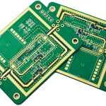
EV Battery PCB: The Complete Guide to Materials, Design, and Manufacturing for Electric Vehicle Battery Management Systems
An EV battery PCB must safely manage 400–800V of pack voltage while maintaining ±2mV cell measurement accuracy over a 15-year automotive lifespan. This guide provides a comprehensive comparison of substrate materials, high-voltage isolation requirements, thermal management strategies, and manufacturing considerations for electric vehicle battery management system PCBs.
Why EV Battery PCBs Are Different From Standard Circuit Boards
Electric vehicle battery management system PCBs operate in an environment that combines high voltage, high current, extreme temperature cycling, and vibration—conditions that quickly destroy standard FR-4 boards. A typical EV BMS PCB must carry sense lines at 400–800V pack voltage with proper creepage and clearance, manage thermal dissipation from balancing resistors dissipating 1–5W per cell, maintain measurement accuracy within ±2mV per cell across -40°C to +85°C, survive 15+ years of thermal cycling in automotive environments, and pass AEC-Q100 and IPC-6012 Class 3 automotive qualification.
Modern electric vehicles are migrating from 400V to 800V electrical architectures—and even 1000V+ systems—to enable ultra-fast charging and reduce cable harnessing weight. Industry analysts estimate that over 40% of new EV platforms launched between 2026 and 2028 will adopt 800V architecture, up from approximately 15% in 2024. This transition has created demanding new requirements for PCB designers: larger creepage and clearance distances, reinforced insulating materials, heavy copper for high-current paths, and advanced thermal management for SiC power electronics.
At gopcba, we specialize in manufacturing EV battery PCBs using a wide range of automotive-grade materials, from high-Tg FR-4 to ultra-high-Tg laminates. Our engineering team has extensive experience in material selection, high-voltage isolation design, heavy copper fabrication, and IATF 16949-compliant manufacturing for electric vehicle applications.
EV Battery PCB Substrate Material Selection
Material selection is the single most critical decision in EV battery PCB design. The substrate must withstand extreme thermal cycling, resist electrochemical migration at high voltages, and maintain mechanical integrity throughout the vehicle’s lifespan. Standard FR-4 materials fail in these environments due to thermal degradation, copper delamination, and Conductive Anodic Filament growth.
High-Tg FR-4: The Entry Point for EV Applications
High-Tg FR-4 materials with glass transition temperatures of 170–180°C represent the baseline for automotive PCBs. These materials offer improved thermal stability over standard FR-4 (Tg ≈ 130–150°C) and can survive the 260°C lead-free reflow process. However, high-Tg FR-4 still struggles with extreme thermal cycling and high-voltage CAF resistance.
For less thermally demanding automotive applications—interior electronics, infotainment, body control modules—a good high-Tg FR-4 may be sufficient. But for battery management systems and powertrain controllers where thermal reliability over a 15-year vehicle lifespan is non-negotiable, more advanced materials are required.
Ultra-High-Tg Laminates: The EV Workhorse
Materials like Nanya NPG-220 represent the top-tier solution for Grade 0 and Grade 1 automotive applications. With a Tg of 220°C (DMA) and a decomposition temperature of 410°C, NPG-220 stays in its rigid, glassy state throughout almost the entire operational and assembly temperature range. This rigidity protects delicate solder joints and microvias from mechanical fatigue.
The Z-axis coefficient of thermal expansion is the most critical metric for long-term reliability. NPG-220 restricts Z-axis expansion to approximately 30–35 ppm/°C before Tg, ensuring that even in 20+ layer boards, the stress on the copper plating remains well within the elastic limit of the copper. This low CTE directly translates into improved plated through-hole fatigue life during thermal cycling.
Isola IS550H: Halogen-Free High-Voltage Protection
Isola IS550H is a halogen-free, ultra-high-reliability thermoset resin system explicitly engineered for heavy copper, high power, and extreme high-voltage applications. Developed in conjunction with a consortium of automotive industry experts, IS550H provides exceptional high-voltage insulation, extreme thermal cycling durability, and environmentally conscious chemistry.
IS550H has been rigorously tested and proven to survive 2000 thermal cycles ranging from -40°C to +175°C. This resilience to thermal shock ensures that the mechanical integrity of the board remains intact throughout the lifespan of the vehicle. The material’s halogen-free formulation eliminates bromine and chlorine typically used as flame retardants, significantly reducing resin polarity and contributing to superior CAF resistance.
Metal-Core and Ceramic Substrates for Extreme Thermal Demands
For applications where organic dielectrics cannot meet thermal or reliability constraints, metal-core PCBs and ceramic substrates offer fundamental material advantages. Insulated Metal Substrates replace the epoxy-glass core with a metal heat spreader, typically aluminum or copper, to enhance heat transfer. Aluminum-based IMS offers thermal conductivity of 1.0–10.0 W/m·K, while copper-based solutions provide even higher bulk conductivity of approximately 390 W/m·K.
Ceramic substrates eliminate the need for an organic polymer interface, providing a direct, inorganic thermal path. Alumina (Al₂O₃) delivers 24–30 W/m·K with a CTE of 4.5–8.0 ppm/°C, making it a stable and cost-effective inorganic solution for power modules. DBC ceramic substrates provide the durability to withstand delamination risks associated with high-current power switching and heavy copper requirements commonly up to 10 oz.
EV Battery PCB Substrate Material Comparison Table
| Material | Tg (°C) | Td (°C) | Z-CTE (ppm/°C) | CAF Resistance | Halogen-Free | Relative Cost | Best For |
|---|---|---|---|---|---|---|---|
| Standard FR-4 | 130–150 | 320–340 | 50–70 | Poor | No | 1× | Non-automotive, low power |
| High-Tg FR-4 (170°C+) | 170–180 | 340+ | 45–55 | Moderate | Varies | 1.2–1.5× | Interior electronics, infotainment |
| Nanya NP-175F | 175 | 340+ | ~50 | Good | No | 2–3× | EV inverters, heavy copper |
| Nanya NPG-170TL | 170 | — | — | Excellent | Yes | 2.5–3.5× | CAF-critical BMS applications |
| Nanya NPG-220 | 220 | 410 | 30–35 | Excellent | Yes | 3–5× | BMS, ADAS, Grade 0/1 automotive |
| Isola IS550H | — | — | — | Superior | Yes | 4–6× | 800V+ high-voltage EV systems |
| Aluminum IMS | N/A | N/A | ~24 | N/A | N/A | 3–8× | High-power LED, IGBT modules |
| Alumina Ceramic | N/A | N/A | 4.5–8.0 | N/A | N/A | 5–10× | SiC inverters, extreme power |
Data compiled from manufacturer datasheets and industry publications.
High-Voltage Isolation Design for EV Battery PCBs
The defining fact of electric vehicle battery management system design is that 400–800V of stacked cell potential has to coexist on or near the same board as 3.3V or 5V digital logic. Every other decision in EV BMS PCB design flows from how cleanly that high-voltage and low-voltage boundary is drawn and enforced.

Creepage and Clearance Requirements
Creepage and clearance provide the surface and air spacing needed to prevent tracking, arcing, and insulation breakdown in high-voltage power modules. For a 400V EV pack, clearance through air must be at least 6.4mm, and creepage along the surface must be at least 8.0mm for Material Group III. For 800V systems, these distances approximately double.
At 800V working voltage, Pollution Degree 2, and standard FR-4 (Material Group IIIa), IEC 60664-1 calls for roughly 8mm of creepage. For 900V DC systems, IPC-2221B recommends a minimum dielectric thickness of no less than 0.8mm, with a base creepage distance of 8.0mm and an altitude correction factor of 1.15 at 2000m, resulting in a final requirement of at least 9.2mm.
In practice, BMS PCBs use routed slots 1.0–1.5mm wide between high-voltage cell connections and low-voltage digital circuitry. These slots effectively multiply the creepage distance without consuming board area proportional to the voltage. High-CTI materials such as Isola 370HR or FR-4 with CTI ≥ 600V are recommended for improved tracking resistance.
Layer Stack for Isolation
A typical isolation stackup places cell connections and balancing circuits on L1 with 2oz copper, a ground plane on L2 as the isolation barrier, digital routing on L3, and low-voltage power and ground on L4. The critical rule is that no copper or via penetrations are allowed in the isolation zone between HV and LV sections. Any via passing through this barrier must maintain the full creepage distance to HV conductors on adjacent layers, typically requiring a via-free keep-out zone of 8+ mm around all high-voltage areas.
Thermal Management for EV Battery PCBs
Passive cell balancing dissipates energy as heat through bleed resistors. For a 12-cell series BMS balancing at 100mA per cell, power per resistor is 3.7V × 100mA = 0.37W, with total balancing power of 12 × 0.37W = 4.44W. Active balancing or higher balancing currents can generate 1–5W per cell. This thermal load concentrated in a small area requires deliberate PCB thermal design.
Thermal Via Arrays
Under each balancing resistor, a thermal via array conducts heat to internal copper planes. Typical specifications include via diameter of 0.3mm (12mil), via pitch of 1.0mm (40mil), array size matching the component footprint, and resin-filled and capped vias for SMT solderability. The target thermal resistance should be below 30°C/W per component.
Copper Weight Selection
L1 cell connections should use 2oz copper minimum for current-carrying traces and thermal spreading. L2 ground plane should use 1–2oz copper as a heat spreader. L3–L4 digital layers can use 1oz standard copper. Heavy copper on L1 serves dual purpose: carrying balancing current without excessive voltage drop and spreading heat from resistors across a larger area for radiation and convection to the enclosure.
For high-current EV applications, heavy copper PCBs typically start at 3oz and can go up to 20oz or more for extreme high-current applications like power converters and EV systems. A single heavy copper layer can replace multiple standard layers, achieving up to 60% space reduction in EV battery management systems.
EV Battery PCB Architecture: Centralized vs. Distributed BMS
A centralized BMS puts all cell monitoring and pack-level control on one board, which simplifies the electronics but means high-voltage sense wiring has to run from every cell tap back to that single board—more HV cable runs, more connector points, more failure modes across a large pack.
The more common approach in modern EV PCB design is modular or distributed: each battery module gets its own cell-monitoring board built around a multi-channel battery monitor IC, and those boards daisy-chain back to a central battery management unit. A 96-cell pack, for example, can be monitored with eight 12-channel battery monitor ICs chained together, each board responsible only for its local module’s cells. This trades simpler, shorter HV wiring for a new requirement: every board-to-board link in the chain now sits at a different absolute voltage relative to the next, which means every one of those links needs its own isolation barrier.
Rigid-Flex Construction for EV Battery PCBs
A modern EV battery pack contains 96–108 cells for 400V systems or 192–216 cells for 800V systems, organized into modules of 8–16 cells each. Each module requires a cell monitoring circuit that connects to the pack-level BMS controller. Traditional approaches using flex cables or wire harnesses with connectors introduce failure points that automotive reliability standards explicitly discourage.
EV BMS PCBs demand rigid-flex construction to connect cell monitoring modules across battery packs while maintaining reliability through -40°C to +85°C thermal cycling. The typical architecture uses 3–6 rigid sections connected by 2–4 flex zones. Each rigid section hosts the cell monitoring IC with its associated passive components, while the flex zones traverse between modules, following the physical geometry of the battery pack structure.
The flex zones must accommodate both static bends and dynamic flex during assembly—the board is flat during SMT, then bent into final configuration during pack assembly. This dual requirement dictates material selection: polyimide base film rated for minimum 500 bend cycles at the installed bend radius, with adhesiveless copper lamination for reliability above 100°C.
Automotive Qualification and Standards for EV Battery PCBs
EV battery PCBs must meet stringent automotive qualification requirements. AEC-Q200 stress testing for passive components has been extended to PCB substrates, requiring temperature cycling from -40°C to +150°C for 1000 cycles minimum. IPC-6012FA, the automotive addendum to the rigid PCB qualification standard, supplements or replaces specific qualification requirements in IPC-6012 to ensure PCBs can withstand vibration and thermal cycling environments in automotive electronic interconnects.
IATF 16949 quality management system certification is a mandatory requirement for automotive OEMs. All 800V EV PCBs must meet UL 94 V-0 flame retardancy rating, with self-extinguishing within 10 seconds. Materials must have a glass transition temperature of at least 170°C for positions adjacent to the engine compartment and inverter. High-CTI materials with CTI greater than 600V provide improved tracking resistance and reliability.
EV Battery PCB Substrate Material Selection Decision Framework
- Step 1: Define operating voltage and temperature range. 400V systems have different creepage requirements than 800V systems. Underhood applications require Tg ≥ 170°C. Powertrain-adjacent PCBs face ambient temperatures of 125–150°C.
- Step 2: Assess thermal cycling requirements. AEC-Q200 qualification requires 1000+ cycles from -40°C to +125°C or +150°C. Materials like Isola IS550H survive 2000 cycles from -40°C to +175°C.
- Step 3: Evaluate CAF resistance requirements. High-voltage DC environments are prone to CAF failure. For 800V+ systems, materials with superior CAF resistance such as NPG-170TL or IS550H are required.
- Step 4: Determine copper weight requirements. BMS current paths typically require 2–5oz copper. High-current paths may require 3–6oz or more.
- Step 5: Consider rigid-flex requirements. Battery pack architectures often require rigid-flex construction to connect distributed cell monitoring modules.
- Step 6: Factor in cost. High-Tg FR-4 costs 1.2–1.5× standard FR-4. Ultra-high-Tg laminates like NPG-220 cost 3–5× standard FR-4. Select the lowest-cost material that meets all performance and qualification requirements.
Frequently Asked Questions About EV Battery PCBs
What is an EV battery PCB?
An EV battery PCB is a printed circuit board used in electric vehicle battery management systems to monitor cell voltages, manage balancing, and ensure safe operation of the battery pack. These boards must handle high voltage (400–800V), high current, and extreme thermal cycling over a 15-year vehicle lifespan.
What materials are used for EV battery PCBs?
EV battery PCBs use automotive-grade materials including high-Tg FR-4 (170–180°C), ultra-high-Tg laminates like Nanya NPG-220 (Tg 220°C), halogen-free materials like Isola IS550H, and for extreme thermal demands, metal-core PCBs or ceramic substrates.
What is the difference between 400V and 800V EV battery PCB requirements?
800V systems require approximately double the creepage and clearance distances of 400V systems. For 800V working voltage at Pollution Degree 2, IEC 60664-1 calls for roughly 8mm of creepage. 800V architectures also demand higher-CTI materials and more robust insulation.
Why is heavy copper used in EV battery PCBs?
Heavy copper (2–5oz or more) is used to carry high balancing currents without excessive voltage drop and to spread heat from balancing resistors across a larger area. Heavy copper also improves thermal management in the confined spaces and high ambient temperatures inside vehicle battery enclosures.
What is CAF resistance and why does it matter for EV battery PCBs?
Conductive Anodic Filament growth is an electrochemical failure where copper ions migrate along fiberglass bundles inside the PCB substrate, bridging high-voltage vias and causing catastrophic internal shorts. High-voltage EV systems (400–800V) are highly prone to CAF failure.
What automotive standards apply to EV battery PCBs?
EV battery PCBs must comply with AEC-Q200 stress testing for temperature cycling, IPC-6012FA automotive addendum for rigid PCBs, IATF 16949 quality management, UL 94 V-0 flame retardancy, and IPC-2221B for creepage and clearance.
What is the cost difference between standard FR-4 and automotive-grade materials?
High-Tg FR-4 typically costs 20–30% more than standard FR-4. Mid-Tg enhanced FR-4 laminates carry a 15–40% premium. Ultra-high-Tg laminates like NPG-220 cost 3–5× standard FR-4.
Key Takeaways for EV Battery PCB Design and Manufacturing
- EV battery PCB material selection is the most critical decision—standard FR-4 fails in automotive high-voltage, high-temperature environments.
- High-Tg FR-4 (170–180°C) is the minimum entry point for automotive applications.
- Ultra-high-Tg laminates like Nanya NPG-220 (Tg 220°C) provide superior Z-axis CTE control (30–35 ppm/°C) for 15-year reliability.
- Halogen-free materials like Isola IS550H offer exceptional CAF resistance for 800V+ systems.
- 800V architectures require approximately double the creepage and clearance of 400V systems.
- Heavy copper (2–5oz or more) is required for current-carrying paths and thermal spreading.
- Rigid-flex construction is mandatory for distributed BMS architectures connecting cell monitoring modules across battery packs.
- AEC-Q200, IPC-6012FA, IATF 16949, and UL 94 V-0 are mandatory automotive qualifications.
- Select the lowest-cost material that meets all performance and qualification requirements for your specific EV application.
Get Expert EV Battery PCB Manufacturing Support
Designing and manufacturing EV battery PCBs requires specialized expertise in material selection, high-voltage isolation, heavy copper fabrication, and automotive qualification. At gopcba, we provide end-to-end EV battery PCB manufacturing services including material selection consulting, DFM analysis, impedance-controlled fabrication, and IATF 16949-compliant assembly.
Our capabilities cover the full spectrum of EV battery PCB requirements—from high-Tg FR-4 and ultra-high-Tg laminates to rigid-flex construction and heavy copper fabrication. We offer prototype PCB assembly, low-volume PCB assembly, and high-volume PCB assembly with rigorous quality control and fast turnaround.
Get a free material selection consultation and DFM analysis for your EV battery PCB project. Contact our engineering team today to discuss your specific requirements and receive expert guidance on the optimal material and design approach for your electric vehicle application.
References
- NextPCB. (2026). Ceramic PCB vs FR4 vs Metal-Core: Substrates for Thermal Management.
- AtlasPCB. (2026). EV Battery Management System PCB: BMS Rigid-Flex Manufacturing Requirements.
- NextPCB. (2026). EV Battery Management System PCB Design: High Voltage Isolation and Layout Rules.
- DEV Community. (2026). EV Battery Management System PCB Design: Thermal Constraints, High-Voltage Isolation, and Manufacturing Specs.
- PCBSync. (2026). Isola IS550H PCB Laminate: Halogen-Free High-Reliability Material for EV Applications.
- PCBSync. (2026). Nanya NPG-220: The Very High-Tg Benchmark for Next-Gen EV and ADAS PCBs.
- PCBSync. (2026). The Engineer’s Guide to Nanya Laminate Automotive ADAS EV PCB Material Selection.
- AtlasPCB. (2026). 800V Electric Vehicle Architecture Driving New PCB Thermal and Insulation Design Requirements.
- AtlasPCB. (2026). Automotive Electronics Reliability Requirements.
- PCBSync. (2025). Heavy Copper PCB Manufacturing: Design Rules, Benefits & Applications Guide.