High-Frequency Impedance PCB Manufacturing: Key Process Requirements
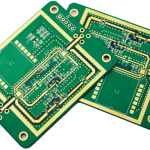
High-frequency impedance PCBs require specialized materials and tightly controlled manufacturing processes to maintain stable signal transmission. Compared with conventional PCBs, these boards demand much stricter control throughout material preparation, lamination, drilling, circuit formation, surface finishing, and final inspection.
The physical structure of a high-frequency board directly affects its electrical characteristics. Variations in dielectric thickness, copper roughness, trace width, layer registration, or material properties can change impedance and increase signal loss. Therefore, every manufacturing stage must be coordinated around the electrical requirements established during design.
1. Material Selection and Pre-Treatment
Material quality is the foundation of stable impedance performance. High-frequency applications generally require low-loss dielectric materials with stable electrical properties across the target frequency range.
The laminate, prepreg, and copper foil must be carefully matched to create a consistent multilayer structure. Depending on the application, specialized RF laminates such as PTFE-based materials, Rogers materials, or other high-performance dielectric systems may be selected.
For high-frequency circuits, copper foil with a low or ultra-low surface profile is often preferred. At high frequencies, the skin effect makes conductor surface roughness increasingly important. A smoother copper surface can help reduce conductor loss and improve signal transmission.
GOPCBA’s PCB Capabilities include high-frequency PCB, RF PCB, controlled-impedance PCB, multilayer PCB, Rogers mixed-lamination PCB, and other advanced PCB technologies.
Incoming materials should also undergo appropriate inspection to verify batch consistency. Storage conditions require controlled temperature and humidity to minimize moisture absorption, oxidation, and dimensional changes before production.
2. Precision Lamination Control
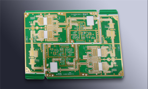
Lamination is one of the most important processes for maintaining consistent dielectric thickness in a multilayer high-frequency impedance PCB.
Standard lamination parameters cannot always be applied to specialized high-frequency materials. The temperature, pressure, heating rate, holding time, and cooling profile should be established according to the selected laminate and prepreg system.
Insufficient pressure may result in voids or poor bonding between layers, while excessive temperature or an unsuitable press cycle can affect the material’s electrical and mechanical properties.
Layer registration is equally important. Any positional deviation between signal layers and reference planes can change the local dielectric geometry and therefore affect impedance.
For this reason, manufacturers need precise lay-up and alignment procedures. Depending on the material structure, vacuum lamination and controlled cooling may also be used to improve bonding consistency and reduce warpage.
For more demanding high-speed applications, PCB Lamination requires careful control of dielectric thickness, resin distribution, layer registration, and material compatibility.
3. Drilling and Hole-Wall Treatment
High-frequency laminates can have significantly different mechanical characteristics from conventional FR-4 materials. Some materials are relatively soft, while ceramic-filled laminates can be considerably harder.
Drilling parameters should therefore be adjusted according to the specific material.
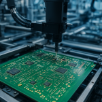
For softer materials, unsuitable drilling conditions may cause burrs, hole deformation, or dimensional instability. Appropriate drill selection, feed rate, spindle speed, and stack height can help reduce mechanical stress during drilling.
Harder filled materials can accelerate drill wear. Tool-life management and scheduled drill replacement are therefore important for maintaining hole diameter and positional accuracy.
When very small holes or microvias are required, laser drilling may provide better dimensional control than conventional mechanical drilling.
After drilling, desmear and hole-wall preparation are required to remove residues and prepare the surface for reliable copper plating. Proper hole-wall treatment is particularly important when vias are part of high-frequency transmission structures.
4. Imaging and Etching Accuracy
Circuit formation directly determines the geometry of high-frequency transmission lines. Trace width, spacing, copper thickness, and edge profile all contribute to impedance performance.
For advanced high-frequency boards, laser direct imaging (LDI) can provide improved pattern accuracy and registration compared with conventional imaging methods.
Etching must also be tightly controlled. Excessive lateral etching can reduce trace width and alter the intended transmission-line geometry. Uneven conductor edges can further increase conductor loss at high frequencies.
Manufacturers should therefore control:
- Trace width
- Trace spacing
- Copper thickness
- Etching compensation
- Side etching
- Line-edge quality
- Layer-to-layer registration
The final conductor geometry should remain within the manufacturing tolerance defined for the impedance calculation.
5. Surface Finish Selection and Control

Surface finish selection should consider both electrical requirements and surface flatness.
For high-frequency impedance boards, a flat and uniform surface finish is generally preferred, particularly when the PCB is used with fine-pitch components or high-speed interconnections.
Common options include ENIG, immersion silver, ENEPIG, and OSP, depending on the application and assembly requirements.
Surface treatment must maintain consistent coating thickness and prevent oxidation, contamination, peeling, or other surface defects.
The appropriate finish should be selected according to the PCB’s electrical performance, assembly process, reliability requirements, and expected service environment.
6. PCB Profile and Final Board Control
The final routing, milling, and profiling processes also require careful control.
High-frequency laminates can be more sensitive to mechanical stress and dimensional deformation. Precision milling tools and appropriate cutting parameters can help reduce chipping, delamination, burrs, and dimensional deviations.
The finished board should be inspected for:
- Board dimensions
- Edge quality
- Warpage
- Surface cleanliness
- Layer integrity
- Delamination
- Copper defects
- Hole quality
- Overall structural consistency
Even relatively small physical defects can become more significant in high-frequency applications because signal performance is closely related to the physical geometry of the transmission path.
7. Impedance Testing and Quality Verification
Manufacturing inspection should verify that the physical PCB matches the electrical requirements defined during design.
For controlled-impedance boards, manufacturers may use impedance coupons and TDR testing to verify actual impedance values. Testing can evaluate whether single-ended or differential transmission structures remain within the specified tolerance.
Important parameters include:
- Trace width
- Copper thickness
- Dielectric thickness
- Dielectric constant
- Reference-plane spacing
- Copper surface roughness
- Layer registration
GOPCBA’s PCB Manufacturing Services support advanced PCB fabrication from prototypes to production, including high-frequency, high-speed, multilayer, HDI, rigid-flex, heavy-copper, and controlled-impedance technologies.
Additional quality-control methods may include AOI, dimensional inspection, cross-section analysis, electrical testing, and other verification procedures according to project requirements.
8. Why Manufacturing and Design Must Be Coordinated

High-frequency impedance performance cannot be controlled by PCB layout alone. The final electrical characteristics depend on the interaction between design geometry, material properties, stack-up construction, and manufacturing tolerances.
For example, impedance is influenced by:
- Trace width
- Trace thickness
- Dielectric thickness
- Dielectric constant
- Copper roughness
- Distance to the reference plane
A small change in any of these parameters can shift the final impedance.
Therefore, engineers should work with the manufacturer before finalizing the stack-up and routing rules. Manufacturer feedback can help ensure that the selected materials, prepreg combinations, copper thicknesses, tolerances, and lamination process are compatible with actual production capabilities.
For complex designs, High-Speed PCB Manufacturing integrates material selection, stack-up engineering, controlled impedance, drilling, plating, DFM review, inspection, and fabrication considerations into a coordinated manufacturing process.
Conclusion
High-frequency impedance PCB manufacturing requires much tighter process control than conventional PCB production. Material selection, copper roughness, dielectric thickness, layer registration, drilling, etching, surface finishing, and final testing can all influence impedance and signal integrity.
A reliable manufacturing process should therefore connect the electrical requirements of the design with the physical realities of fabrication.
By combining appropriate High-Frequency PCB Materials, precise PCB Lamination, accurate circuit formation, controlled impedance, and comprehensive inspection, manufacturers can reduce signal loss, minimize impedance variation, and improve the reliability of high-frequency electronic systems.
For advanced RF, microwave, 5G, radar, networking, and high-speed computing applications, a manufacturer with proven high-frequency and controlled-impedance capabilities can provide more reliable support from prototype development through production. GOPCBA’s published capabilities include high-frequency PCB, RF materials, controlled impedance, multilayer construction, HDI, blind and buried vias, and other advanced PCB technologies.