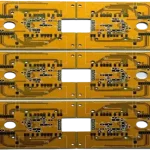
40-Layer Any-Layer Interconnect PCB Solution
A 40-layer PCB is designed for high-performance electronic systems that require extremely high wiring density, stable signal integrity, and reliable power distribution. By combining high layer counts, any-layer interconnect technology, precision microvia fabrication, and advanced multilayer lamination, this type of board can support demanding applications such as AI servers, high-performance computing, telecommunications, and advanced industrial equipment.
Unlike conventional multilayer structures, an Any-layer Interconnect PCB allows electrical connections to be established between different layers through microvia structures. This reduces routing restrictions, improves space utilization, and provides greater flexibility for complex high-density circuit designs.
For projects requiring advanced fabrication from prototype to volume production, our PCB Manufacturing Services support multilayer, HDI, high-speed, high-frequency, rigid-flex, controlled-impedance, and other specialized PCB technologies.
Core Architecture and Layer Stackup
The 40-layer structure uses alternating copper layers and dielectric materials to create a mechanically stable multilayer construction. The internal layers can be organized according to their electrical functions, including signal, power, and ground layers.
A carefully engineered stackup helps separate high-speed signals from power distribution networks while providing stable reference planes for controlled-impedance routing. Symmetrical layer arrangement is also important for minimizing mechanical stress and reducing the risk of board warpage during fabrication.
The any-layer interconnect structure eliminates many of the routing limitations associated with conventional through-hole vias and traditional sequential blind-via structures. Microvias can provide direct connections between selected layers, reducing unnecessary layer transitions and freeing additional routing space.
For complex high-density designs, PCB Design & Layout Services can support stackup development, impedance calculations, multilayer design, HDI structures, blind and buried vias, and manufacturability analysis.
Key Manufacturing Processes
Precision Drilling and Layer Interconnection
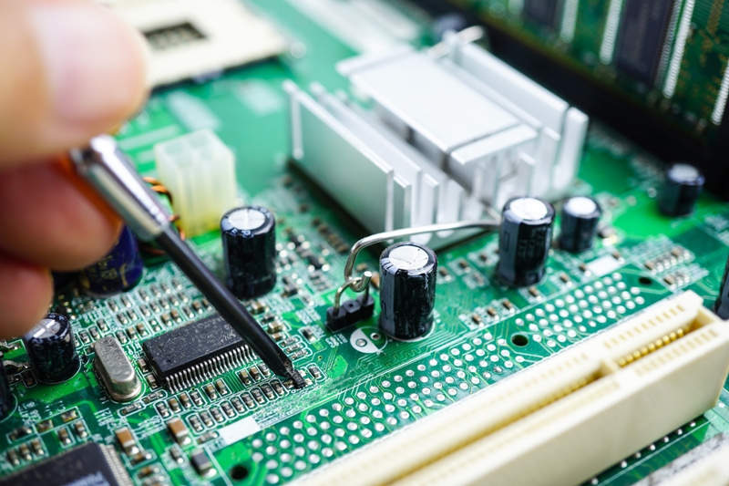
Laser drilling is used to create small microvias for high-density interconnection. Advanced laser-drilling processes can produce microvia structures suitable for compact HDI and high-layer-count designs.
Copper plating and via filling are then used to establish reliable electrical connections between layers. Proper control of hole geometry, copper deposition, via filling, and layer registration is essential for maintaining long-term interconnection reliability.
For an HDI PCB, microvia diameter, capture-pad size, aspect ratio, stacking method, copper thickness, and lamination sequence should all be evaluated together rather than treated as independent design parameters.
Fine-Line Circuit Formation
High-density routing requires precise control of trace width and spacing. Fine-line imaging and etching processes help create compact circuit patterns while maintaining dimensional consistency.
For high-speed designs, trace geometry directly affects impedance and signal integrity. Trace width, copper thickness, dielectric thickness, dielectric constant, and reference-plane distance should therefore be considered together during stackup and routing development.
Multilayer Vacuum Lamination
Lamination is one of the most critical processes in a High-Layer-Count PCB.
Multiple copper layers and dielectric materials must be bonded into a mechanically stable structure. Temperature, pressure, heating and cooling rates, resin flow, lamination time, and layer registration all require precise process control.
Vacuum lamination can help reduce trapped air and promote more uniform pressure throughout the multilayer stack. For complex high-layer-count structures, stable lamination is essential for controlling warpage, internal voids, delamination, and layer misalignment.
Material Selection and Electrical Performance
Material selection has a direct impact on the electrical performance of high-speed multilayer boards.
Depending on the application, PCB construction may use enhanced FR-4, high-TG materials, mid-loss laminates, low-loss materials, PTFE-based materials, or hybrid material structures.
For demanding high-speed applications, low-loss dielectric materials can help reduce signal attenuation and maintain signal quality over critical transmission paths. Hybrid stackups can also combine different materials to balance electrical performance, manufacturing complexity, and cost.
For more information about material selection and advanced structures, our High-Speed PCB Manufacturing solutions cover stackup engineering, low-loss materials, impedance control, microvias, sequential lamination, and other high-speed manufacturing requirements.
Electrical Performance and Signal Integrity
Controlled Impedance
High-speed interfaces require consistent transmission-line geometry. A controlled-impedance design should account for:
- Trace width
- Copper thickness
- Dielectric thickness
- Dielectric constant
- Reference-plane spacing
- Copper surface characteristics
For demanding applications, impedance targets should be established during stackup development rather than after routing has already been completed.
TDR testing, impedance coupons, cross-section analysis, and dimensional measurements can be used to verify whether the manufactured PCB meets the specified electrical requirements.
Crosstalk Reduction
With dozens of signal layers, crosstalk can become an important design consideration.
Dedicated ground planes and carefully arranged signal layers can shorten return-current paths and provide better electromagnetic isolation between adjacent circuits. Appropriate spacing between critical signal traces can further reduce unwanted coupling.
A well-designed multilayer stackup should therefore balance routing density with signal integrity rather than simply maximizing the number of available routing channels.
Power Distribution
High-performance processors and computing systems can generate substantial power demand. A multilayer PCB can use dedicated power and ground planes to create a lower-impedance power distribution network.
Continuous reference planes also provide stable return paths for high-speed signals and help reduce power noise and electromagnetic interference.
Applications of 40-Layer PCB Technology
A 40-layer PCB is particularly suitable for systems where board space, routing density, signal speed, and power requirements are all demanding.
Typical applications include:
- AI servers and accelerator systems
- High-performance computing platforms
- High-speed networking equipment
- 5G and next-generation communication infrastructure
- RF and microwave equipment
- Semiconductor testing equipment
- Advanced industrial control systems
- High-speed computing backplanes
For AI computing applications, high-layer-count structures can provide additional routing channels for processors, memory, power delivery, networking interfaces, and other high-density components. Our AI Server PCB Manufacturing solutions cover high-layer-count, high-speed, HDI, high-frequency, high-TG, and controlled-impedance PCB technologies.
Why Choose Any-Layer Interconnect Technology?
Compared with conventional multilayer PCB construction, Any-layer Interconnect PCB technology provides several important advantages for advanced electronic systems.
Higher Routing Density
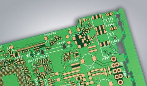
Microvias allow connections to be established between selected layers without requiring every connection to pass through the entire board. This increases available routing space and supports more compact layouts.
Shorter Electrical Paths
Direct layer-to-layer interconnections can reduce unnecessary via transitions and electrical path length. This can be particularly useful for high-speed signal routing.
Better BGA Breakout
Fine-pitch BGA devices can create significant routing challenges. Microvias and via-in-pad structures can provide more efficient escape routing around high-density component packages.
Greater Design Flexibility
Any-layer structures give engineers greater freedom when assigning signal, power, and ground layers. This can simplify complex interconnections while allowing the stackup to be optimized for signal integrity and power integrity.
Manufacturing Considerations
A high-layer-count PCB should be designed around the manufacturer’s validated process window.
Before production, engineers should confirm:
- Layer count and final board thickness
- Material availability
- Stackup configuration
- Minimum trace and spacing
- Microvia diameter
- Via filling requirements
- Sequential lamination requirements
- Layer registration capability
- Controlled-impedance requirements
- Surface finish
- Electrical testing requirements
- Prototype-to-production compatibility
High-layer-count manufacturing introduces additional process complexity. Early engineering review can identify potential problems with registration, lamination, drilling, copper distribution, thermal expansion, and manufacturability before production begins.
High-Layer-Count PCB Manufacturing for Advanced Electronics
A 40-layer any-layer interconnect structure combines high routing density, advanced microvia technology, precision multilayer lamination, and controlled electrical performance. It provides a practical PCB architecture for electronic systems that require more interconnection capacity than conventional multilayer boards can provide.
For AI computing, telecommunications, high-speed networking, RF equipment, and semiconductor systems, the combination of 40-layer PCB, Any-layer Interconnect PCB, High-Layer-Count PCB, HDI PCB, and High-Speed PCB technologies can help engineers address increasing requirements for density, signal integrity, power delivery, and system integration.
GOPCBA provides PCB fabrication and assembly services from engineering review and prototyping through production manufacturing, supporting advanced multilayer, HDI, high-speed, high-frequency, rigid-flex, and controlled-impedance PCB requirements.