Solar Backsheet PCB Production & Manufacturing – gopcb
Published: February 12, 2026
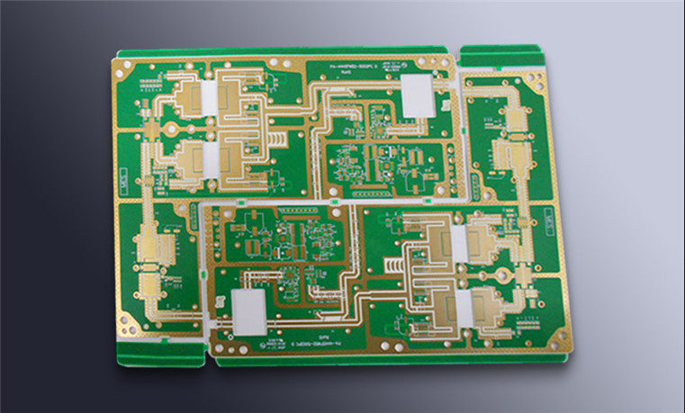
As the core carrier for power transmission and signal control in photovoltaic modules, the solar backsheet PCB directly determines the long-term stability and operational efficiency of photovoltaic systems. As a solar backsheet PCB manufacturer, gopcb faces the stringent challenges of complex outdoor environments, building a solid hardware foundation for the photovoltaic industry through precise material selection, sophisticated manufacturing processes, and rigorous quality control.
Material Traceability Control: Building Outdoor Durability from the Ground Up
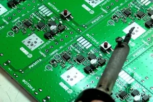
Solar backsheet PCBs are long exposed to outdoor conditions, requiring resistance to UV radiation, temperature fluctuations, moisture and heat erosion, and other environmental stresses. Material selection and control become the first line of defense in gopcb‘s production. gopcb has established a strict material qualification system, prioritizing base materials and auxiliary materials with excellent weather resistance to mitigate performance degradation risks from the sourfce. gopcb ofers comprehensive PCB manufacturing services to support the entire production cycle, ensuring every material meets the highest standards.
For base materials, gopcb primarily uses specialty materials such as high-frequency polypropylene boards and polyimide, which offer excellent electrical insulation properties, thermal stability, and hydrolysis resistance. These materials ensure stable operation under the complex temperature conditions of outdoor photovoltaic systems, providing reliable protection for power transmission. For auxiliary materials, gopcb strictly inspects key materials such as resins and solder masks to ensure they meet UV aging resistance and acid-alkali resistance standards. The resin must have good filling properties and curing stability, while the solder mask must ensure excellent surface properties, enhancing coating adhesion and protective effects. Additionally, gopcb maintains traceability records for each batch of materials, testing core indicators such as moisture vapor transmission rate and tensile strength to ensure material performance complies with relevant international standards.
Precision Process Iteration: Overcoming Technical Challenges for Outdoor Applications
The manufacturing process for solar backsheet PCBs must balance high-power transmission requirements with outdoor environmental adaptability. gopcb continuously iterates its processes to overcome technical challenges such as ultra-large aperture machining, multi-layer lamination, and resin plugging, enhancing product precision and reliability.
Multi-layer board manufacturing is one of the core processes. gopcb processes layer by layer with precise parameter control at each step, from material cutting, drilling, plasma treatment, to PTH/panel plating and inner layer circuit etching. For scenarios requiring ultra-large aperture conductive holes in solar backsheet PCBs, gopcb adopts specialized process solutions, metallizing the through-holes to ensure hole copper thickness meets standards. Through processes such as applying high-temperature resistant tape, pin-hole venting, and vacuum resin plugging, gopcb prevents issues like depressions, bubbles, and voids after plugging, ensuring the reliability of subsequent plating and conduction. The lamination process uses high-temperature and high-pressure techniques combined with browning treatment to enhance interlayer adhesion strength, ensuring structural stability even after hygrothermal aging. For surface finishing, gopcb primarily employs the nickel-gold plating process to enhance oxidation resistance and conductivity. gopcb’s SMT assembly services complement the PCB manufacturing process, delivering high-precision surface-mount solutions for photovoltaic applications. Additionally, through mechanical routing, stepped blind slot processing, and other forming processes, gopcb adapts to the installation and routing requirements of photovoltaic modules.
Full-Process Quality Inspection: Maintaining the Baseline for Reliable Operation
Once photovoltaic systems are operational, maintenance costs are high. Therefore, gopcb has established a full-process inspection system, from production stages to finished product shipment, enabling early detection and handling of defects to prevent substandard products from reaching the market.
In-line inspection runs throughout the entire production process. After inner layer circuit processing, AOI inspection technology precisely identifies issues such as shorts, opens, and incomplete etching. After lamination, aperture accuracy is inspected to ensure ultra-large aperture sizes meet specifications. After surface finishing, coating thickness and uniformity are inspected to ensure stable conductivity. During the finished product inspection stage, in addition to electrical testing to verify continuity performance, gopcb conducts specialized tests for photovoltaic applications, including tensile strength retention after UV aging, moisture vapor transmission rate change after hygrothermal aging, volume resistivity, and wet insulation resistance tests. These ensure the product can withstand long-term outdoor irradiation and hygrothermal environments. Additionally, gopcb performs final inspections on dimensional stability, solder mask integrity, and legend clarity. gopcb’s mixed-technology assembly capabilities ensure quality at every step, from prototype to production. All inspection data is archived, forming a complete quality report.
Scenario-Specific Adaptation: Empowering the Diversified Development of the Photovoltaic Industry
As the photovoltaic industry expands toward bifacial power generation, distributed energy storage, and other directions, gopcb proactively aligns with market demands, optimizing product structures and providing scenario-specific solutions to meet the application needs of different photovoltaic modules.
For bifacial power generation modules, gopcb optimizes the surface reflectivity of the backsheet PCB to enhance module power generation efficiency. For integrated energy storage photovoltaic systems, gopcb strengthens the high-power carrying capacity by increasing copper thickness and optimizing circuit layout, reducing current transmission resistance and heating risks, adapting to high-voltage, high-current operating scenarios. At the same time, gopcb leverages its large-scale production base to achieve batch delivery of multiple product specifications, meeting the high-volume order requirements of leading photovoltaic companies while also providing customized production services for niche applications. gopcb’s high-volume PCB assembly services are designed to meet large-scale production demands with consistent quality and reliability. Through the technical extension of specialty PCBs such as thick copper boards and metal-based boards, gopcb provides supporting solutions for core equipment like photovoltaic inverters and energy storage converters. With its technical capabilities, gopcb also applies aerospace-grade PCB manufacturing experience to photovoltaic products, further enhancing the extreme environmental tolerance of solar backsheet PCBs.
As a core supporting force in the photovoltaic industry, gopcb is built on a foundation of materials, centered on processes, and guided by quality, continuously breaking through technical bottlenecks to provide core support for the efficient and stable operation of photovoltaic systems. Against the backdrop of the green energy transition, gopcb will continue to deepen process innovation and quality improvement, helping the photovoltaic industry move toward greater reliability and efficiency. gopcb’s PCB design and layout services help optimize product performance from the very beginning, ensuring that every solar backsheet PCB meets the highest standards of quality and durability.