High-Speed PCB Manufacturer for Signal Integrity Testing
As high-speed electronic applications continue to expand, Signal Integrity has become a critical factor in determining system stability, transmission accuracy, and overall performance. As the primary carrier for electrical signals, a PCB must provide stable electrical characteristics and precise physical structures throughout the transmission path.
For high-speed applications, PCB manufacturing quality directly affects impedance consistency, transmission loss, crosstalk, reflection, and other signal-related characteristics. Although a PCB manufacturer is primarily responsible for fabricating the board, comprehensive process control is essential for providing a reliable hardware foundation for subsequent signal integrity testing and system verification.
For projects requiring advanced fabrication capabilities, GOPCBA provides a range of PCB Manufacturing Services covering high-speed, high-frequency, multilayer, HDI, and controlled-impedance PCB requirements.
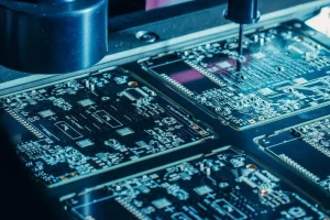
High-speed signals traveling through a PCB are sensitive to impedance discontinuities, transmission loss, crosstalk, reflections, and other electrical effects. Many of these problems are closely related to PCB manufacturing accuracy. Therefore, manufacturers need to establish strict process controls around critical production stages to minimize potential signal-integrity risks from the beginning.
For a Controlled Impedance PCB, trace width, trace spacing, copper thickness, dielectric thickness, and material properties must be carefully controlled. Even small dimensional variations can change the characteristic impedance of a transmission line.
At high frequencies and data rates, impedance discontinuities may cause signal reflections, ringing, overshoot, undershoot, and waveform distortion. Manufacturers therefore need accurate imaging and etching processes together with reliable inspection methods to maintain consistent trace geometry.
The dielectric thickness between a signal layer and its reference plane is equally important. Variations in dielectric thickness can affect the electromagnetic field distribution around the transmission line and consequently change impedance. Controlled lamination processes are therefore necessary to maintain a stable multilayer structure.
Copper surface roughness is another factor that should be considered in high-speed PCB manufacturing. As signal frequency increases, current tends to concentrate near the conductor surface. Excessive copper roughness can increase conductor loss and contribute to higher insertion loss. For demanding applications, manufacturers should therefore select suitable copper foil and maintain appropriate surface characteristics throughout fabrication.
Via structures also have a significant influence on high-speed signal transmission. A via introduces parasitic inductance and capacitance into the signal path. If the drilling position, hole diameter, pad size, or surrounding clearance is poorly controlled, the via can create an impedance discontinuity.
High-density and high-speed boards may require blind vias, buried vias, microvias, or other advanced interconnection structures. These structures require accurate drilling, plating, registration, and inspection.
For multilayer applications, via spacing should also be considered carefully. Insufficient clearance between vias, traces, pads, or copper planes can create both manufacturing and electrical problems. Engineers can refer to GOPCBA’s Multilayer PCB Via Spacing design guidance when developing high-density layouts.
Manufacturers should use appropriate drilling technologies and inspection procedures to control hole diameter, hole position, annular ring dimensions, and interlayer registration. Properly designed antipads and sufficient clearance from reference planes can further reduce unwanted parasitic effects.
PCB material selection has a direct influence on high-speed transmission performance. Different applications require different combinations of dielectric constant, dielectric loss, thermal stability, dimensional stability, and mechanical strength.
For demanding High-Frequency PCB applications, low-loss materials with stable electrical characteristics may be required to reduce dielectric loss and signal attenuation. Standard FR-4 materials can be suitable for many conventional digital applications, but higher-speed or higher-frequency systems may require more specialized material systems.
Material selection should therefore consider:
GOPCBA’s Multilayer PCB Material Selection guidance covers the differences between standard FR-4, high-frequency materials, and thermally enhanced material systems.
A reliable manufacturing process should include incoming material inspection and production traceability. Material specifications should be verified before production to ensure that the selected laminate, copper foil, prepreg, and other materials meet the approved requirements.
For high-speed applications, variations in Dk and Df can influence impedance and transmission loss. Thermal expansion and moisture absorption can also affect dimensional stability during manufacturing and operation.
The glass-fiber structure of a laminate deserves additional attention. In certain high-speed designs, the distribution of glass fibers relative to signal traces can contribute to local variations in effective dielectric properties. Engineers and manufacturers can reduce these effects through appropriate stack-up planning, routing strategies, material selection, and lamination control.
A carefully designed Multilayer PCB stack-up provides a controlled environment for high-speed signal transmission. The arrangement of signal layers, ground planes, power planes, and dielectric materials determines the return-current path, electromagnetic field distribution, impedance, and crosstalk behavior.
For high-speed designs, signal layers should generally be positioned close to continuous reference planes. A short and predictable return path helps reduce loop area and minimizes unwanted electromagnetic radiation.
For example, a six-layer high-speed structure may include signal, ground, high-speed signal, power, ground, and signal layers. However, there is no universal stack-up that fits every design. The appropriate structure depends on data rate, impedance requirements, layer count, material characteristics, copper thickness, routing density, and manufacturing capability.
GOPCBA’s High-Speed PCB Stack-Up Design guidance provides additional information about signal layers, reference planes, power distribution, and impedance considerations for high-speed multilayer designs.
A well-controlled stack-up can provide:
PCB manufacturers may not always perform the complete system-level signal integrity analysis, but the fabricated PCB must provide a reliable physical platform for subsequent testing.
Before signal integrity measurements are performed, basic electrical inspection should be completed to identify open circuits, short circuits, incorrect connections, and other manufacturing defects. Otherwise, basic PCB defects may interfere with test results and lead to incorrect conclusions.
For production projects, representative samples can be provided for advanced verification methods such as TDR, eye-diagram analysis, insertion-loss measurements, return-loss measurements, and S-parameter testing.
Time-domain reflectometry (TDR) can help identify impedance discontinuities along a transmission path. When a signal encounters a change in impedance, part of the signal is reflected. By analyzing the reflected waveform, engineers can identify potential discontinuities associated with traces, vias, connectors, or transitions between PCB layers.
For a Controlled Impedance PCB, TDR testing can therefore provide useful feedback on whether the manufactured transmission structures are consistent with the intended design.
If testing reveals unexpected impedance deviations, the manufacturer can investigate potential causes such as trace-width variation, dielectric-thickness variation, copper-thickness variation, lamination changes, or material inconsistencies.
Eye-diagram analysis provides a visual representation of signal quality and can reveal problems such as excessive jitter, attenuation, inter-symbol interference, and insufficient timing margin.
S-parameter measurements provide additional information about high-frequency transmission behavior. Parameters such as insertion loss and return loss can help engineers evaluate the performance of transmission channels across a specified frequency range.
Although these measurements are typically performed as part of system or channel validation, PCB manufacturing data can provide valuable background information for interpreting the results.
Manufacturers should therefore maintain records covering trace dimensions, layer thickness, laminate type, copper weight, via specifications, stack-up structure, and other relevant production parameters.
As data rates increase, PCB manufacturing tolerances become increasingly important. High-density designs often require smaller trace widths and tighter spacing, increasing the potential for crosstalk and manufacturing variation.
Manufacturers must therefore continuously improve imaging, etching, lamination, drilling, plating, and inspection processes.
For complex High-Speed PCB designs, layer-to-layer registration is particularly important. Misalignment between internal copper patterns, vias, pads, and reference planes can affect both electrical performance and manufacturing yield.
High-speed boards may also use HDI structures and microvias to support dense routing. These structures require precise drilling, plating, stacking, and registration capabilities.
GOPCBA’s PCB Capabilities provide information about manufacturing tolerances, microvia structures, dielectric thickness, copper features, and other fabrication capabilities relevant to high-density PCB production.
A mature PCB manufacturing process should maintain a comprehensive process database covering materials, equipment parameters, dimensional measurements, electrical test results, and production lots.
By correlating manufacturing parameters with electrical performance, manufacturers can identify recurring process deviations and optimize production conditions more efficiently.
For example, if impedance measurements show a consistent deviation from the target value, engineering teams can investigate whether the issue originates from trace geometry, dielectric thickness, copper thickness, material characteristics, or lamination parameters.
This data-driven approach creates a closed-loop manufacturing process:
Design → Engineering Review → Manufacturing → Inspection → Testing → Analysis → Process Optimization
Such a process helps improve repeatability and provides better control over high-speed PCB production.
The ultimate objective of signal integrity testing is to verify whether a signal can travel through the complete transmission channel with acceptable levels of distortion, loss, reflection, and noise.
However, signal integrity cannot be separated from PCB manufacturing quality. Trace geometry, dielectric thickness, copper roughness, via structures, layer registration, material characteristics, and stack-up configuration all influence the electrical behavior of the final board.
For this reason, high-speed PCB manufacturing should be treated as an integrated engineering process rather than simply a board fabrication activity.
A manufacturer with appropriate process capabilities can help engineers translate the intended electrical design into a physically consistent PCB structure. This is particularly important for high-speed computing, networking, telecommunications, automotive electronics, industrial control, test equipment, and other applications where transmission performance is critical.
Reliable Signal Integrity begins with a PCB structure that can maintain predictable electrical characteristics throughout the transmission path.
For high-speed applications, manufacturers need to focus on impedance control, material selection, stack-up design, via quality, lamination accuracy, layer registration, inspection, and manufacturing consistency. These factors work together to create a stable hardware foundation for subsequent TDR, eye-diagram, S-parameter, and system-level signal integrity testing.
As electronic systems continue to move toward higher data rates and greater routing density, the requirements for High-Speed PCB, High-Frequency PCB, Controlled Impedance PCB, and Multilayer PCB manufacturing will continue to increase.
By combining precise fabrication, appropriate materials, controlled processes, advanced inspection, and continuous process optimization, PCB manufacturers can provide more consistent circuit boards and help engineers achieve reliable high-speed signal transmission in demanding electronic systems.