PCB Back Drilling Technology for Multilayer PCBs
A Multilayer PCB is a critical platform for modern electronic systems, and its signal transmission quality directly affects overall equipment performance. Through-holes are essential structures for establishing electrical connections between different PCB layers. However, conventional through-holes can leave unused copper sections, commonly known as via stubs, which may cause signal reflection, attenuation, resonance, and crosstalk during high-frequency and high-speed transmission.
PCB Back Drilling provides an effective solution to this problem. By precisely removing the redundant portion of a plated through-hole, back drilling shortens the unwanted electrical path and improves signal transmission characteristics. As a result, it has become an important manufacturing technology for advanced multilayer boards used in 5G communications, data centers, aerospace systems, and other high-performance electronic applications.
What Is PCB Back Drilling?
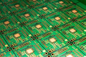
PCB Back Drilling, also known as controlled-depth drilling, is a precision secondary drilling process used to remove redundant portions of plated through-holes in multilayer PCBs.
In a conventional multilayer board, a through-hole generally extends through the entire thickness of the PCB. However, a signal may only need to connect specific layers rather than the entire board. The unused section of the plated through-hole beyond the required connection forms a via stub.
During the Back Drilling Process, a drill with a slightly larger diameter than the original through-hole is used from the designated side of the PCB. The drilling depth is precisely controlled so that the redundant copper stub is removed while the portion required for electrical connection remains intact.
The main purpose is to create a shorter and cleaner signal path, reducing unwanted electrical discontinuities while maintaining the mechanical and electrical reliability of the remaining interconnection.
Why Do Through-Hole Stubs Affect High-Speed Signals?
In high-frequency and high-speed circuits, an unused via stub can behave as an unwanted transmission-line branch. As signal frequency and data rates increase, the stub can contribute to signal reflection, resonance, insertion loss, and crosstalk.
These effects may result in:
- Signal distortion
- Timing jitter
- Eye-diagram closure
- Increased insertion loss
- Higher bit error rates
- Reduced high-speed transmission stability
For this reason, controlling via geometry and interconnection structures is an important part of Signal Integrity engineering.
By physically removing the redundant stub, back drilling can reduce unwanted electrical discontinuities and create a more controlled signal path. This makes it particularly valuable for high-speed and high-frequency PCB designs.
For complex boards, back drilling should also be considered together with PCB stack-up, via structures, impedance requirements, and overall manufacturing capability. GOPCBA provides advanced Multilayer PCB fabrication for complex PCB structures and high-density applications.
Multilayer PCB Manufacturing
PCB Back Drilling Process
Back drilling is not an independent manufacturing step. It is integrated into the overall multilayer PCB production workflow and must be coordinated with inner-layer fabrication, lamination, primary drilling, hole metallization, and subsequent PCB processing.
A typical Back Drilling Process can be divided into four major stages.
1. Preliminary Multilayer PCB Manufacturing
Before back drilling begins, the basic multilayer PCB structure must first be completed.
The inner-layer circuits are fabricated and inspected before the cores and prepreg materials are stacked according to the designed layer structure. The layers are then laminated to form a complete multilayer board.
After lamination, the primary drilling process creates the through-holes required for interlayer electrical connections.
The drilled holes then undergo hole-wall treatment and metallization. Electroless copper is deposited onto the hole walls, followed by electrolytic copper plating to achieve the required conductive thickness.
This plated through-hole structure provides the electrical connection that will later be partially modified by back drilling.
The broader PCB Manufacturing Process includes circuit formation, drilling, copper plating, solder mask application, surface finishing, electrical testing, and final inspection.
PCB Manufacturing Process
2. Precision Back Drilling Operation
The back drilling stage is the core of the technology and mainly involves accurate positioning and controlled-depth drilling.
Precision Positioning
A high-precision CNC drilling system identifies PCB reference points and plated through-hole locations. Coordinate compensation is then applied to ensure that the back-drill tool is correctly aligned with the target hole.
Accurate positioning is essential because excessive deviation can damage the effective copper connection or leave part of the unwanted stub behind.
Controlled-Depth Drilling
After positioning, the drilling system controls the depth according to the layer connection requirements.
The drill enters from the designated side and stops near the target connection layer while maintaining an appropriate process margin. The objective is to completely remove the redundant copper stub without damaging the copper structure that remains electrically active.
The back-drill diameter is generally slightly larger than the original through-hole diameter so that the redundant plated section can be completely removed.
During drilling, process parameters must also be controlled to minimize copper burrs, resin debris, and other contaminants that could affect subsequent manufacturing operations.
3. Cleaning and Inspection After Back Drilling
After PCB Back Drilling is completed, the drilled area must be thoroughly cleaned to remove copper particles, resin dust, and other debris.
High-pressure cleaning and appropriate hole-cleaning procedures can help prevent contamination from affecting subsequent electrical connections or PCB manufacturing processes.
Inspection should then verify:
- Back-drill depth
- Remaining stub length
- Hole position
- Hole-wall condition
- Effective copper-layer integrity
If the remaining stub is excessive, additional processing may be required. If over-drilling damages an effective copper layer, the board may require rework or rejection depending on the severity of the defect.
Accurate inspection is therefore an important part of PCB manufacturing quality control.
4. Subsequent PCB Manufacturing Processes
After back drilling and inspection are completed, the multilayer PCB continues through the remaining manufacturing stages.
These processes may include:
- Outer-layer pattern formation
- Additional copper plating
- Solder mask application
- Legend printing
- Surface finishing
- Electrical testing
- PCB routing and profiling
During subsequent copper processing, the back-drilled area must maintain reliable electrical and mechanical characteristics.
For advanced boards, process coordination is particularly important because the back-drilled structure interacts with the PCB stack-up, copper thickness, hole geometry, and high-speed signal requirements.
Key Benefits of PCB Back Drilling
The use of PCB Back Drilling provides several important benefits for advanced multilayer PCB applications.
Improved Signal Integrity
Improving Signal Integrity is the primary reason for implementing back drilling.
Removing the unused through-hole stub reduces unwanted signal reflection and resonance. It can also help reduce insertion loss and crosstalk, particularly in high-speed transmission channels.
By creating a more controlled electrical path, back drilling can support stable transmission at higher data rates and improve the overall performance of high-speed interfaces.
Improved PCB Reliability
Redundant stubs can also contribute to unwanted structural stress and contamination-related risks within the through-hole structure.
Removing the unused section can reduce unnecessary structural features and help create a cleaner interconnection structure.
When combined with appropriate cleaning, inspection, and quality-control procedures, back drilling can contribute to improved mechanical and electrical stability throughout the operating life of the PCB.
Support for High-Density PCB Design
As electronic products become smaller and more integrated, PCB designs increasingly require higher layer counts, smaller geometries, and denser interconnections.
Back drilling allows designers to retain the basic advantages of plated through-holes while removing unnecessary portions of the hole structure.
This makes the technology particularly useful for advanced Multilayer PCB designs where high routing density and high-speed transmission must coexist within a compact board structure.
PCB Back Drilling for High-Speed Applications
The electrical benefits of back drilling become increasingly important as signal frequencies and data rates rise.
A High-Speed PCB may contain multiple high-speed interfaces operating simultaneously. At these data rates, even relatively small discontinuities in the transmission path can influence signal quality.
Back drilling can therefore be used together with:
- Controlled impedance
- Optimized PCB stack-up
- Appropriate dielectric materials
- Accurate trace geometry
- Stable reference planes
- Proper via design
- High-precision manufacturing
For high-speed multilayer designs, stack-up and impedance control should be considered together with via structures and manufacturing tolerances. GOPCBA provides technical guidance for high-speed PCB stack-up, reference planes, and impedance control.
High-Speed PCB Stack-Up Design
Applications of PCB Back Drilling
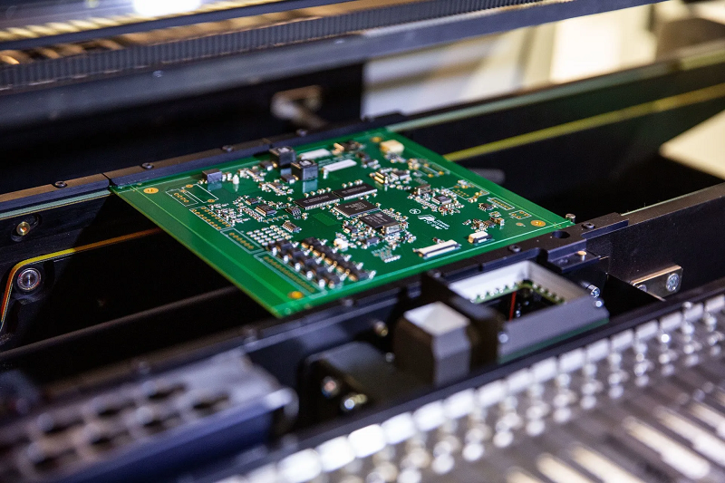
Because of its ability to improve high-speed transmission performance, back drilling is commonly used in applications where signal integrity and reliability are critical.
5G Communication Equipment
5G base stations, routers, optical modules, and other communication equipment transmit high-speed and high-frequency signals.
The through-hole structures used in these systems can introduce unwanted signal discontinuities. Back drilling helps reduce the effects of redundant stubs and supports cleaner high-speed signal paths.
For 5G and other high-frequency applications, PCB material selection, impedance control, multilayer construction, and fabrication tolerances must work together to maintain stable signal transmission.
Data Centers and Servers
Servers, switches, and other data-center equipment rely on high-speed interfaces for data transmission.
Signal distortion and excessive insertion loss can negatively affect system performance. Back-drilled multilayer boards can help reduce unnecessary discontinuities in high-speed channels and support more stable data transmission.
This makes the technology suitable for high-speed server motherboards, networking equipment, optical-module interfaces, and related hardware.
Aerospace and Avionics
Aerospace systems such as radar, satellite communication equipment, and advanced avionics require high reliability and stable high-frequency signal transmission.
A High-Speed PCB used in these systems must maintain predictable electrical characteristics under demanding operating conditions.
Back drilling can help optimize interconnections and reduce unwanted signal effects, making it a useful technology for advanced aerospace PCB manufacturing.
High-End Consumer Electronics
High-performance graphics cards, laptops, smartphones, and other advanced consumer electronics increasingly require compact multilayer boards with high routing density and fast interfaces.
Back drilling can help optimize signal paths within dense PCB structures while supporting the high-speed transmission requirements of modern processors, memory, communication interfaces, and other components.
Back Drilling and PCB Design
Back drilling should be considered during PCB design rather than treated solely as a manufacturing adjustment.
The PCB stack-up, via structure, target connection layers, drill diameter, back-drill diameter, remaining stub length, dielectric thickness, and signal requirements should be evaluated together.
For high-speed applications, the interconnection design should also be coordinated with impedance control and return-current paths.
A properly designed multilayer stack-up helps maintain continuous reference planes and predictable signal paths. When a high-speed signal changes layers through a via, its return current must also have an appropriate transition path.
For this reason, back drilling should be evaluated as part of the complete high-speed PCB design rather than as an isolated manufacturing operation.
GOPCBA’s multilayer PCB design guidance covers stack-up, power planes, ground planes, vias, and signal-integrity considerations for advanced PCB designs.
Multilayer PCB Design and Signal Integrity
Quality Control for Back-Drilled PCBs
Because back drilling directly affects the electrical geometry of a PCB, manufacturing inspection is essential.
Important quality-control items include:
- Drill position accuracy
- Back-drill depth
- Remaining stub length
- Hole-wall quality
- Copper thickness
- Layer registration
- Electrical continuity
- Final board dimensions
Back drilling should be performed within controlled manufacturing tolerances. Excessive drilling depth can damage an active copper layer, while insufficient depth can leave too much of the redundant stub and reduce the intended signal-integrity benefit.
For high-performance boards, the back-drilling process should therefore be integrated with broader PCB Quality Control, including process inspection and electrical testing.
PCB Quality Control and Manufacturing Reliability
Conclusion
Through-hole back drilling is an important precision technology for advanced multilayer PCB manufacturing. By selectively removing redundant through-hole stubs, it can shorten unwanted electrical paths, reduce signal reflection and resonance, and improve Signal Integrity in high-speed transmission systems.
A reliable Back Drilling Process requires accurate positioning, controlled drilling depth, appropriate tool selection, thorough cleaning, and precise inspection. It must also be coordinated with lamination, drilling, plating, PCB stack-up, impedance control, and electrical testing.
As 5G communications, data centers, aerospace electronics, high-performance computing, and advanced consumer electronics continue to demand faster and denser signal transmission, PCB Back Drilling will remain an important manufacturing technology for high-performance Multilayer PCB and High-Speed PCB applications.