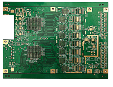
With the rapid development of microelectronic technology, electronic products are continuously moving toward miniaturization, higher integration, and increased functionality. As a result, the manufacturing requirements for High-Precision Multilayer PCB have become increasingly strict. Modern electronic devices require PCBs with finer circuits, smaller vias, higher layer counts, and more complex interconnection structures.
Among all PCB Manufacturing processes, copper plating is one of the most critical steps because it directly affects electrical connection reliability between PCB layers. However, as PCB designs continue to advance toward high-density interconnect structures, traditional vertical electroplating technology faces limitations in achieving uniform copper deposition inside high aspect ratio holes and microvias.
To overcome these challenges, Horizontal Electroplating technology has been developed as an advanced copper deposition method. Compared with conventional vertical plating, horizontal electroplating provides better solution circulation, improved copper distribution, and enhanced reliability for advanced multilayer PCB applications.
As an experienced PCB manufacturer, Kingda continuously improves advanced manufacturing processes and plating technologies to support the production of high-performance electronic products. This article introduces the working principles, system structure, process advantages, and development trends of horizontal electroplating technology.
1. Challenges of Traditional PCB Electroplating Technology
With the continuous development of High-Precision Multilayer PCB technology, PCB structures are becoming increasingly complex. Modern designs require smaller hole diameters, narrower line spacing, finer circuits, and higher-density interconnections.
For advanced multilayer boards, the aspect ratio of through holes may exceed 5:1, while deep blind vias are widely used in HDI PCB manufacturing. These structures create significant challenges for traditional vertical electroplating processes.
During vertical copper plating, the current distribution inside the hole is usually uneven. The current density near the hole entrance and edge area is higher, while the current gradually decreases toward the center of the hole.
This uneven distribution causes several problems:
- Excessive copper deposition around the hole opening
- Insufficient copper thickness inside deep holes
- Poor plating uniformity
- Potential reliability issues during long-term operation
Although manufacturers can improve deep-hole plating performance by adjusting current density, adding chemical additives, increasing solution agitation, and applying cathode movement technology, these methods become less effective when PCB structures continue to shrink.
Therefore, Horizontal Electroplating technology was developed to provide better plating performance for advanced PCB applications.
2. Working Principle of Horizontal Electroplating Technology
Horizontal Electroplating is an advanced plating technology developed from traditional vertical electroplating methods. Unlike vertical systems where PCB panels are placed vertically, horizontal electroplating positions the PCB parallel to the plating solution surface.
During the process:
- The PCB acts as the cathode.
- Conductive rollers provide electrical connection and panel transportation.
- The plating solution flows evenly across the PCB surface.
- Copper ions are deposited uniformly into holes and microvias.
The horizontal solution flow improves electrolyte exchange inside holes, allowing copper ions to reach deeper areas more effectively. This helps achieve better copper coverage and improves the reliability of through-hole structures.
The technology is especially suitable for:
- High-Precision Multilayer PCB
- HDI PCB
- Fine-pitch circuit boards
- High-reliability electronic products
3. Basic Structure of Horizontal Electroplating System
A complete Horizontal Electroplating system mainly consists of several key components, including the transportation system, electrode system, electrolyte circulation system, filtration system, and automatic control system.
3.1 PCB Transportation and Conductive System
In a horizontal plating system, PCB panels are transported through conductive rollers. These rollers provide electrical connection while also controlling PCB movement through different plating stages.
The conductive rollers are designed with flexible structures to accommodate different PCB thicknesses. During operation, however, copper deposition may occur on the roller surface because the rollers are exposed to the plating solution.
Therefore, modern equipment designs include:
- Replaceable conductive components
- Automatic cleaning systems
- Easy maintenance structures
These improvements help maintain stable production performance and reduce equipment downtime.
3.2 Electrode System Design
The electrode system plays an important role in controlling copper deposition quality.
Modern horizontal plating equipment usually uses insoluble titanium anodes combined with copper materials. The distance between the anode and PCB surface must be carefully controlled to maintain stable current distribution.
Proper electrode design helps achieve:
- Uniform copper thickness
- Stable plating efficiency
- Improved hole filling performance
- Reduced surface defects
For advanced PCB Manufacturing, accurate electrode control is essential for achieving consistent product quality.
3.3 Electrolyte Circulation and Filtration System
The circulation system is one of the most important parts of horizontal electroplating equipment.
A pump and nozzle system continuously circulates plating solution across the PCB surface. The controlled liquid flow creates turbulence around holes, improving:
- Copper ion transportation
- Chemical additive distribution
- Gas removal
- Deep-hole plating capability
A filtration system is also installed to remove particles generated during plating. Maintaining clean plating solution helps prevent contamination defects and improves PCB Reliability.
4. Advantages of Horizontal Electroplating in PCB Manufacturing
Compared with traditional vertical plating methods, Horizontal Electroplating provides several advantages for modern PCB production.
4.1 Improved Copper Thickness Uniformity
The horizontal solution flow reduces uneven current distribution and improves copper deposition consistency inside holes.
This is especially important for:
- High-layer-count PCBs
- High-density interconnect boards
- Advanced electronic packaging applications
4.2 Better High Aspect Ratio Hole Plating Capability
As PCB designs become smaller and more complicated, high aspect ratio holes become increasingly common.
Horizontal electroplating improves electrolyte exchange inside deep structures, allowing better copper filling performance and reducing the risk of incomplete plating.
4.3 Higher Process Stability and Production Efficiency
Modern horizontal plating systems use automated control technology to monitor and adjust important parameters, including:
- Current density
- Conveyor speed
- Solution temperature
- Chemical concentration
- Pump flow rate
Automatic process control improves production consistency and helps manufacturers achieve stable quality during mass production.
5. Process Control Requirements
To achieve reliable Copper Plating Process results, manufacturers must carefully control multiple production parameters.
Important factors include:
- PCB thickness
- Hole diameter
- Aspect ratio
- Required copper thickness
- Current density
- Solution circulation speed
- Chemical additive concentration
- Temperature control
For high-end HDI PCB manufacturing, precise process monitoring is essential to ensure electrical performance and mechanical reliability.
Kingda evaluates PCB structure, material selection, production requirements, and application conditions to optimize plating processes for different customer requirements.
Conclusion
As electronic products continue developing toward higher integration and miniaturization, the requirements for High-Precision Multilayer PCB manufacturing continue to increase.
Traditional vertical electroplating technology has limitations when processing high aspect ratio holes and advanced interconnection structures. Horizontal Electroplating technology provides an effective solution by improving electrolyte circulation, copper distribution, and process stability.
Through advanced equipment design, accurate process control, and professional manufacturing experience, Kingda helps customers achieve reliable and high-performance PCB products.
In the future, with the continuous development of HDI technology, semiconductor packaging, and high-density electronic systems, horizontal electroplating will continue to play an important role in advanced PCB Manufacturing processes.