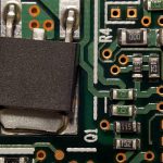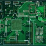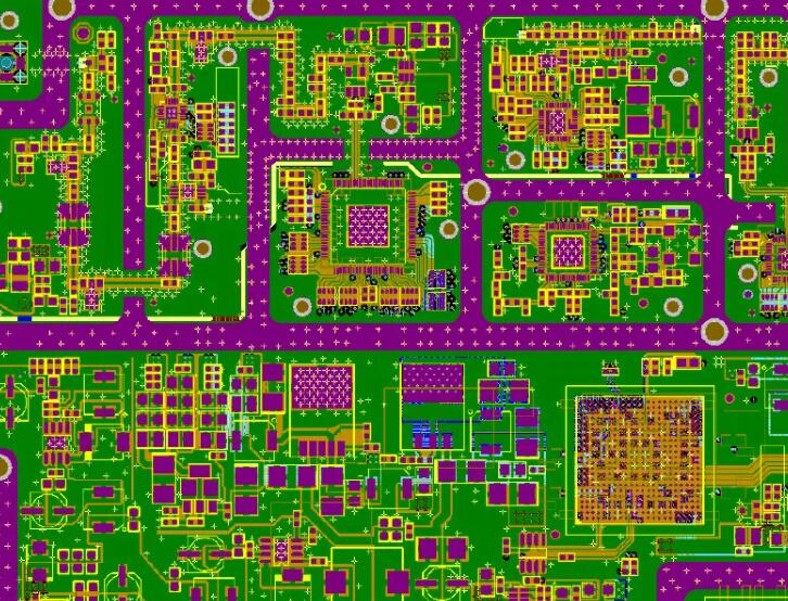
As electronic products continue to evolve toward miniaturization, higher performance, and greater integration, SMT assembly has become one of the most important technologies in modern electronics manufacturing. Compared with traditional through-hole assembly, surface mount technology offers significant advantages in component density, electrical performance, production efficiency, automation, and overall manufacturing cost.
At the same time, selecting appropriate PCB materials is essential for achieving the required mechanical strength, electrical performance, thermal stability, and reliability of a printed circuit board. This article introduces the major advantages of SMT chip processing and provides an overview of common PCB substrate materials.
Advantages of SMT Chip Processing and Packaging
1. Smaller Electronic Equipment and Higher Component Density
One of the most significant advantages of SMT chip processing is its ability to substantially reduce the size and weight of electronic products.
Compared with conventional through-hole components, surface-mount components are generally much smaller and lighter. Their compact packages allow more components to be placed within the same PCB area, significantly increasing assembly density.
With the development of fine-pitch packaging, component pitches have evolved from relatively large traditional dimensions to 1.27 mm, 0.8 mm, 0.65 mm, 0.5 mm, and even finer pitches for advanced packages.
Because SMT components are mounted directly onto the PCB surface, they do not require long component leads or large through-holes. This allows designers to use both sides of the PCB more efficiently and significantly improve component placement density.
As a result, surface mount technology can help reduce the overall size and weight of electronic equipment while supporting increasingly complex circuit functions.
2. High Reliability and Strong Vibration Resistance
SMT assembly uses compact surface-mount components that are directly soldered to PCB pads. Their short electrical connections and relatively low component mass provide good mechanical stability.
Compared with traditional through-hole components, SMT assemblies generally have fewer mechanical protrusions and shorter electrical paths. This can improve resistance to vibration and mechanical shock when the PCB is properly designed and assembled.
Automated SMT production also provides highly consistent component placement and soldering conditions. With appropriate process control, solder-joint defect rates can be kept very low.
The combination of automated placement, controlled solder paste printing, accurate component positioning, and controlled reflow soldering makes SMT assembly particularly suitable for high-volume and high-reliability electronic products.
Today, surface-mount technology is widely used across consumer electronics, communications equipment, automotive electronics, industrial control systems, medical devices, and other electronic products.
3. Better High-Frequency Performance and Signal Integrity
Another important advantage of surface mount technology is improved high-frequency electrical performance.
Traditional through-hole components often have relatively long leads. These leads introduce parasitic inductance and capacitance, which can affect high-frequency signal transmission.
Surface-mount components have much shorter electrical connections. When combined with appropriate PCB layout and controlled impedance routing, this can reduce parasitic effects and improve high-frequency characteristics.
This is particularly important for high-speed digital circuits, RF circuits, communication systems, and other applications where signal integrity is critical.
However, the maximum operating frequency of a PCB assembly is not determined by the package type alone. PCB stack-up, trace geometry, dielectric properties, return-current paths, component package structure, and power integrity all influence high-frequency performance.
Therefore, SMT assembly should be considered together with appropriate PCB design and signal-integrity engineering.
4. Higher Production Efficiency and Automated Manufacturing
SMT chip processing is highly compatible with automated electronics manufacturing.
Modern pick-and-place machines use vacuum nozzles and precision motion systems to automatically pick up and place components onto PCB pads. Because surface-mount components are placed directly on the PCB surface, the placement process can be highly automated.
Compared with conventional through-hole insertion, SMT eliminates many mechanical insertion operations and supports high-speed component placement.
Modern SMT production lines can integrate:
- Solder paste printing
- 2D/3D solder paste inspection
- High-speed component placement
- Fine-pitch component placement
- Reflow soldering
- Automated optical inspection (AOI)
- X-ray inspection
- Electrical testing
This high level of automation improves production consistency, reduces manual intervention, and supports high-volume PCB assembly.
Fine-pitch components such as QFP, QFN, BGA, and other advanced packages can also be processed efficiently when the PCB design and manufacturing process are properly controlled.
5. Lower Manufacturing and Overall Product Costs
Although the initial investment in SMT production equipment can be significant, SMT assembly can reduce overall manufacturing costs through higher production efficiency and material utilization.
The major cost advantages include:
Reduced PCB size:
Because SMT allows much higher component density, designers can often achieve the same functionality on a smaller PCB.
Fewer drilled holes:
Unlike through-hole assembly, most SMT components do not require component-lead holes. This can simplify PCB fabrication and reduce drilling requirements.
Lower assembly labor:
Highly automated SMT production reduces manual component insertion and soldering operations.
Reduced packaging and logistics costs:
Smaller and lighter components and PCBs can reduce packaging, transportation, and storage requirements.
Lower rework and inspection costs:
Automated placement and inspection systems can improve process consistency and help detect defects earlier.
Overall, the economic benefits of SMT depend on product volume, component mix, PCB complexity, equipment utilization, and manufacturing process design.
PCB Substrate Materials Classification
The PCB substrate is the fundamental structural material used to manufacture a printed circuit board. It provides mechanical support and contributes significantly to the electrical, thermal, and reliability characteristics of the finished PCB.
A typical PCB substrate consists primarily of resin, reinforcement material, and copper foil.
Common resin systems include epoxy resin, phenolic resin, polyester resin, BT resin, and polyimide resin. Reinforcement materials may include paper or fiberglass.
The conductive layer is generally copper foil, which can be produced using different manufacturing methods and selected according to the PCB application.
1. Classification by Reinforcement Material
Paper-Based PCB Substrates
Paper-based substrates are commonly used in cost-sensitive and relatively low-performance electronic products.
Typical grades include FR-1, FR-2, and FR-3, depending on the resin system and performance requirements.
These materials generally offer good machinability and low cost but have more limited thermal and electrical performance compared with high-performance fiberglass-reinforced materials.
Glass-Fiber-Reinforced Epoxy Substrates
FR-4 is one of the most widely used PCB substrate materials.
It uses fiberglass reinforcement combined with epoxy resin and provides a good balance of mechanical strength, electrical insulation, thermal performance, manufacturability, and cost.
FR-4 materials are widely used in consumer electronics, industrial equipment, communication systems, computers, automotive electronics, and many other applications.
For higher-performance applications, enhanced FR-4 and other high-Tg materials may be selected to provide improved thermal reliability.
Composite Substrates
Composite materials combine different reinforcement structures or material systems to achieve specific performance and cost requirements.
Common examples include CEM-1 and CEM-3.
CEM materials can provide a balance between cost, mechanical performance, and electrical characteristics and are often used in applications where standard FR-4 performance is not required.
HDI PCB Materials
HDI PCB structures require specialized dielectric materials and manufacturing processes to support microvias, fine lines, fine spacing, and high interconnection density.
Resin-coated copper (RCC) and other thin dielectric materials can be used in HDI construction.
The material selection must consider dielectric thickness, dimensional stability, thermal expansion, laser-drilling performance, copper adhesion, and reliability during repeated thermal cycles.
For advanced PCB manufacturing, material selection and PCB stack-up design should be evaluated together with the required HDI structure.
Special PCB Substrate Materials
Certain applications require specialized substrate materials rather than conventional FR-4.
Examples include:
- Metal-core substrates
- Ceramic substrates
- High-frequency and low-loss laminates
- Flexible polyimide substrates
- Thermally conductive materials
- High-temperature materials
These materials are selected according to application-specific requirements such as thermal conductivity, dielectric loss, dimensional stability, operating temperature, flexibility, and mechanical strength.
2. Classification by Flame Retardancy
PCB substrates can also be classified according to their flame-retardant performance.
Common classifications include:
- UL94 V-0
- UL94 V-1
- UL94 HB
The specific material grade should be selected according to the safety requirements of the end product and applicable industry standards.
For many electronic products, flame-retardant materials are required to reduce the risk of ignition and flame propagation.
3. Classification by Resin System
Different resin systems provide different combinations of thermal, mechanical, electrical, and chemical properties.
Phenolic Resin PCB
Phenolic resin substrates are generally economical and are commonly used in relatively simple, low-cost electronic products.
Epoxy Resin PCB
Epoxy resin is widely used in PCB manufacturing, particularly in fiberglass-reinforced FR-4 materials.
It provides good mechanical strength, electrical insulation, chemical resistance, and thermal performance.
Polyester Resin PCB
Polyester resin materials can be used in certain PCB applications where cost and specific mechanical characteristics are important.
BT Resin PCB
BT resin, or bismaleimide-triazine resin, provides improved thermal performance and dimensional stability compared with conventional epoxy systems.
It is commonly associated with advanced packaging and high-density electronic applications.
Polyimide PCB
Polyimide resin has excellent thermal resistance and flexibility.
It is widely used in flexible printed circuits, high-temperature applications, and certain rigid-flex PCB structures.
How to Select the Right PCB Materials
Selecting PCB substrate materials should not be based solely on price.
Engineers should evaluate several factors, including:
- Operating temperature
- Glass transition temperature (Tg)
- Decomposition temperature (Td)
- Coefficient of thermal expansion (CTE)
- Dielectric constant (Dk)
- Dissipation factor (Df)
- Thermal conductivity
- Mechanical strength
- Moisture resistance
- PCB thickness and layer count
- High-speed signal requirements
- Manufacturing process compatibility
For high-speed and high-density designs, dielectric properties and dimensional stability become particularly important. For power electronics and LED applications, thermal conductivity may be a major consideration.
Therefore, choosing the appropriate PCB materials should be based on the complete electrical, mechanical, thermal, and manufacturing requirements of the product.
Conclusion
SMT chip processing and advanced PCB manufacturing technologies have become essential to modern electronics production.
Compared with traditional through-hole assembly, surface mount technology provides significant advantages in component density, automation, high-frequency performance, reliability, and manufacturing efficiency.
At the same time, the selection of appropriate PCB substrate materials directly affects the electrical performance, thermal stability, mechanical strength, manufacturability, and long-term reliability of the PCB.
Kingda can provide PCB manufacturing and assembly solutions for a wide range of applications, helping customers select suitable materials, PCB structures, and manufacturing processes according to their product requirements.
By combining appropriate PCB materials, optimized PCB design, controlled SMT assembly, and reliable manufacturing processes, manufacturers can achieve smaller, more efficient, and more reliable electronic products.