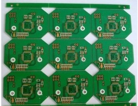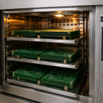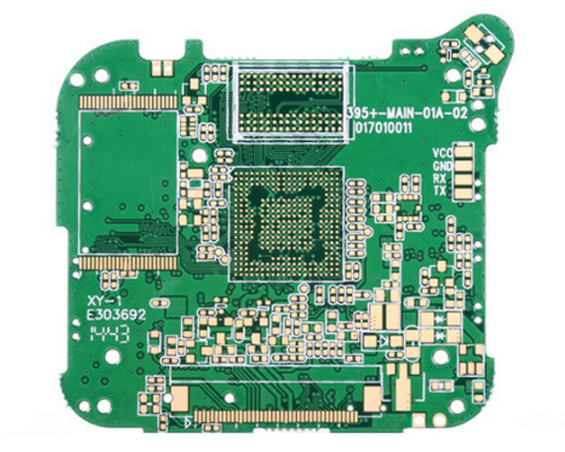
Before starting mass production of a new PCB, PCB Prototyping is an important step for verifying design feasibility, manufacturing capability, product performance, and production quality.
A prototype is more than a preliminary sample. It provides an opportunity to identify design and manufacturing risks before committing to a larger production volume. Through prototype fabrication and testing, engineers can evaluate whether the PCB design can be manufactured consistently and whether the selected materials, dimensions, vias, pads, and other structures are suitable for the intended application.
At the same time, prototype production provides an opportunity for customers and the PCB Manufacturer to confirm technical requirements, manufacturing tolerances, inspection methods, and production specifications before mass production begins.
Why Is PCB Prototyping Important?
PCB Prototyping can provide valuable information before large-scale production. It helps reduce manufacturing risks and establishes a reliable foundation for subsequent production.
1. Evaluate PCB Manufacturer Capability
When working with a new supplier, prototype production provides a practical way to evaluate the manufacturer’s technical and manufacturing capabilities.
A prototype can reveal whether the manufacturer can consistently meet requirements for:
- Board dimensions
- Layer count
- Trace width and spacing
- Hole diameter
- Via structure
- Copper thickness
- Layer registration
- Surface finish
- Impedance control
- PCB flatness
- Electrical testing
A supplier may claim a particular manufacturing capability, but actual production performance is better evaluated through representative prototype boards.
For demanding designs, the prototype should ideally use the same or similar materials, stackup, copper thickness, and critical geometries planned for mass production.
This allows the customer to evaluate not only whether the board can be produced, but also whether the manufacturing process is stable enough for long-term production.
2. Reduce Defects During Mass Production
The manufacturing process of a PCB includes multiple stages, such as imaging, etching, drilling, lamination, copper plating, solder mask application, surface finishing, and electrical testing.
Each stage can introduce potential variation.
PCB Prototyping allows these potential problems to be identified at a relatively small production volume.
Typical prototype verification may include:
- Visual inspection
- Dimensional inspection
- Cross-sectional analysis
- Electrical continuity testing
- Insulation resistance testing
- Via inspection
- Copper thickness measurement
- Solderability evaluation
- Impedance testing for controlled-impedance designs
Once critical problems have been identified and corrected, the manufacturing process can be transferred to mass production with greater confidence.
However, prototype success does not automatically guarantee zero defects in mass production. Process capability and statistical control should continue to be monitored during volume production.
3. Establish a Foundation for Mass Production
A successful PCB Prototype can provide useful engineering data for future production.
During prototype manufacturing, engineers can evaluate:
- Material selection
- Stackup structure
- Trace geometry
- Via dimensions
- Manufacturing tolerances
- Surface finish
- Thermal performance
- Signal integrity
- Assembly compatibility
This information can then be used to optimize the design before production volume increases.
Prototype validation can also identify opportunities to reduce unnecessary manufacturing complexity and control production costs.
For example, a via diameter that is unnecessarily small may require specialized drilling equipment and increase fabrication costs. Increasing the via size slightly, when electrically and mechanically acceptable, may improve manufacturing yield and reduce cost.
4. Confirm Design and Manufacturing Requirements
Successful PCB production requires close communication between the PCB designer and the PCB Manufacturer.
Before beginning PCB Prototyping, both parties should confirm important technical information, including:
- Gerber or ODB++ files
- NC drill files
- Stackup information
- Material specifications
- Copper thickness
- Surface finish
- Controlled impedance requirements
- Board thickness
- Via specifications
- Special fabrication requirements
- Testing requirements
The manufacturer should also review the design for manufacturability.
This Design for Manufacturability (DFM) review can identify potential problems before fabrication begins.
PCB Via Size Requirements
As PCB technology develops toward higher density, smaller form factors, and greater electrical performance, via dimensions have become increasingly important.
A via provides an electrical connection between different PCB layers. Its size affects routing density, manufacturability, current-carrying capability, drilling reliability, and cost.
Common PCB via structures include:
- Through-hole vias
- Blind vias
- Buried vias
- Microvias
The appropriate structure depends on the PCB stackup and interconnection requirements.
What Determines PCB Via Size?
There is no single universal via size suitable for every PCB.
PCB Via Size should be determined by several factors, including:
- PCB thickness
- Hole diameter
- Finished hole size
- Drill diameter
- Copper plating thickness
- Aspect ratio
- Current requirements
- Component pitch
- Routing density
- Manufacturer capability
- Required production yield
- Cost considerations
Therefore, via dimensions should be established together with the PCB fabrication process rather than selected independently during layout.
Finished Hole Size vs. Drill Size
One important point in PCB design is the difference between the finished hole diameter and the mechanical drill diameter.
The drill diameter used during fabrication may be larger than the required finished hole because copper plating is subsequently deposited on the hole wall.
For example, if a design specifies a particular finished hole diameter, the PCB manufacturer may select an appropriate drill diameter based on the expected plating thickness and process capability.
Therefore, designers should clearly distinguish between:
Finished Hole Size and Drill Tool Size
when defining manufacturing data.
Through-Hole Via Design
Through-Hole Vias extend through the entire PCB and are commonly used to connect multiple conductive layers.
They are generally easier to manufacture than extremely small microvias, but they consume more routing area because the via extends through all layers.
A larger hole may also require a larger pad and greater clearance from surrounding copper.
When designing through-hole vias, engineers should consider:
- Finished hole diameter
- Pad diameter
- Annular ring
- Clearance from copper planes
- Board thickness
- Aspect ratio
- Current requirements
- Drill reliability
Via Aspect Ratio
The aspect ratio is an important consideration in PCB drilling.
A simplified definition is:
Aspect Ratio = PCB Thickness ÷ Finished Hole Diameter
For example, a thicker PCB with a very small hole has a higher aspect ratio and is more difficult to drill and plate reliably.
As the aspect ratio increases, challenges may include:
- Drill quality
- Hole-wall cleanliness
- Desmear effectiveness
- Electroless copper coverage
- Copper plating uniformity
- Hole reliability
Therefore, a small via diameter should not be selected without considering the total PCB thickness.
Why Smaller Vias Are More Difficult to Manufacture
As electronic products become smaller and more integrated, designers increasingly use smaller vias to save routing space.
For example, a design may require a via smaller than 0.3 mm because of fine-pitch components or dense routing.
However, reducing the hole diameter increases manufacturing difficulty.
Potential challenges include:
- Smaller mechanical drill diameter
- Greater drill breakage risk
- Reduced drilling process margin
- More demanding hole-wall treatment
- More difficult copper plating
- Higher inspection requirements
- Lower manufacturing yield
For extremely small interconnects, laser-drilled microvias may be more appropriate than conventional mechanical through-holes.
When Should a 0.3 mm Via Be Used?
A finished hole diameter around 0.3 mm is commonly achievable for many conventional PCB manufacturing processes, but it should not be regarded as a universal minimum or standard.
Whether a manufacturer can reliably produce a 0.3 mm finished hole depends on:
- Board thickness
- Material construction
- Aspect ratio
- Drill technology
- Plating process
- Production volume
- Equipment condition
- Required yield
If the design uses a very thick PCB with a very small hole, the aspect ratio may become excessive even though the hole itself appears reasonable.
Therefore, designers should communicate the required finished hole size and board thickness with the PCB Manufacturer before finalizing the design.
Via Size and Current-Carrying Capability
Via diameter is also related to current-carrying capability.
A larger via generally provides a larger conductive cross-sectional area and can provide more robust current transfer, particularly when copper plating thickness is considered.
For power applications, designers should not determine via diameter based solely on routing density.
They should also evaluate:
- Current
- Temperature rise
- Copper plating thickness
- Number of parallel vias
- Via spacing
- Thermal requirements
When higher current is required, multiple vias may be used in parallel instead of relying on a single small via.
Via Size and PCB Routing Density
A smaller via can save valuable routing space, especially in high-density PCB designs.
However, reducing via diameter may also reduce the manufacturing process window.
Therefore, the smallest possible via is not always the best solution.
A better approach is to select the smallest practical via that satisfies the electrical, mechanical, and manufacturing requirements.
This approach can improve:
- Manufacturing yield
- Cost efficiency
- Reliability
- Process stability
- Production scalability
Mechanical Vias vs. Microvias
For conventional multilayer boards, mechanical through-hole vias are commonly used.
For high-density interconnect applications, microvias may be used to create shorter interconnections and free routing space on inner layers.
Microvias are generally produced using laser drilling and are typically associated with HDI structures.
Their design requires additional consideration of:
- Laser-drilling capability
- Microvia diameter
- Dielectric thickness
- Copper thickness
- Stacked or staggered structures
- Sequential lamination
- Reliability requirements
Therefore, HDI via design should be evaluated together with the entire stackup and manufacturing process.
PCB Via Pad and Annular Ring
The relationship between the via hole and its surrounding copper pad is another important design consideration.
The annular ring provides a margin of copper around the finished hole.
An insufficient annular ring can increase the risk of breakout caused by drilling or registration variation.
When designing small vias, engineers should consider:
- Finished hole size
- Pad diameter
- Drill tolerance
- Layer registration
- Etching tolerance
- Plating requirements
As via dimensions become smaller, manufacturing tolerances become increasingly important.
PCB Prototyping and Via Verification
During PCB Prototyping, critical via structures should be verified before moving into mass production.
Depending on the application, verification may include:
- Hole diameter measurement
- Cross-sectional analysis
- Plated-hole inspection
- Copper thickness measurement
- Electrical continuity testing
- Thermal stress testing
- Reliability testing
For high-reliability multilayer boards, cross-sectional analysis can provide valuable information about hole-wall quality, plating thickness, annular ring, and interlayer connections.
Common PCB Prototyping Mistakes
Designing to the Absolute Minimum Capability
Using the smallest hole or narrowest trace that a manufacturer can theoretically produce may leave little process margin.
A design should consider production yield rather than only nominal capability.
Ignoring Board Thickness
A small hole in a thin PCB may be relatively easy to manufacture, while the same hole in a thick multilayer board may create a challenging aspect ratio.
Failing to Specify Finished Hole Size
Confusing drill size with finished hole size can lead to incorrect manufacturing data.
Overusing Small Vias
Smaller vias are not automatically better. If a larger via can meet the electrical requirements, it may provide better manufacturing stability and lower cost.
Skipping Prototype Verification
Moving directly from a first design to mass production can increase the risk of discovering manufacturing problems after significant production costs have already been incurred.
Best Practices for PCB Prototyping
For a successful PCB Prototype, consider the following practices:
- Confirm manufacturing capabilities before PCB layout.
- Establish realistic trace, spacing, and via dimensions.
- Specify finished hole sizes clearly.
- Evaluate the PCB aspect ratio.
- Consider current requirements when selecting via dimensions.
- Use DFM analysis before fabrication.
- Verify critical dimensions during prototype production.
- Perform cross-sectional analysis when appropriate.
- Confirm surface finish and material specifications.
- Document prototype results before mass production.
- Maintain the same critical materials and stackup between prototype and production whenever possible.
- Review any design changes introduced after prototype validation.
Kingda’s Approach to PCB Prototyping
At Kingda, PCB Prototyping is treated as an important engineering stage between PCB design and mass production.
Our approach focuses on evaluating the relationship between PCB design requirements and actual manufacturing capabilities.
For projects involving multilayer structures, fine-line routing, small vias, controlled impedance, or high-density interconnections, key manufacturing parameters can be reviewed before production.
These may include:
- PCB material selection
- Layer stackup
- Copper thickness
- Trace width and spacing
- Via dimensions
- Drilling requirements
- Layer registration
- Surface finish
- PCB thickness
- Electrical testing
- Reliability requirements
By identifying potential manufacturing risks during the prototype stage, customers can make informed design adjustments before committing to higher production volumes.
Conclusion
PCB Prototyping is an important step in PCB development because it provides an opportunity to verify design feasibility, manufacturing capability, product performance, and process stability before mass production.
At the same time, PCB Via Size should be selected according to the complete design and manufacturing requirements rather than a fixed industry-wide value.
Factors such as PCB thickness, finished hole diameter, aspect ratio, copper plating, current requirements, routing density, drilling technology, and manufacturing capability all influence the appropriate via size.
For conventional multilayer boards, Through-Hole Vias remain widely used. For high-density designs, smaller mechanical vias or laser-drilled microvias may provide greater routing flexibility.
The best PCB design is not necessarily the one that uses the smallest possible features. Instead, it is a design that balances electrical performance, mechanical reliability, manufacturing yield, cost, and long-term production stability.
By combining effective PCB Design, practical PCB Manufacturing requirements, and systematic prototype verification, manufacturers and designers can reduce production risks and establish a stronger foundation for reliable mass production.