PCB Copper Thickness Control: Ensuring Stable Current Carrying Capacity in PCB Manufacturing
In PCB manufacturing and electronic applications, copper layer thickness is one of the most important factors determining electrical performance and reliability. Stable PCB Copper Thickness Control ensures that current can flow efficiently through circuits without excessive heat generation, voltage loss, or premature aging caused by insufficient copper thickness.
As electronic devices continue to develop toward higher power density, smaller sizes, and more complex functions, the requirements for PCB Current Carrying Capacity are becoming increasingly demanding. Uneven copper thickness may result in localized current concentration, increased resistance, signal interference, and potential circuit failures.
Effective control of PCB Copper Layer Thickness is not achieved through a single production step. Instead, it requires precise management throughout copper deposition, etching, surface treatment, and inspection processes. By maintaining consistent copper thickness across the entire board, manufacturers can improve electrical stability, product reliability, and long-term performance.
Copper deposition is a critical stage in PCB Manufacturing, as it directly determines the final copper thickness of circuit layers. The stability of the electroplating and chemical copper deposition processes has a significant impact on copper uniformity.
During the electroless copper plating process, unstable chemical conditions may cause different copper deposition rates across the PCB surface. Some areas may accumulate excessive copper, while other regions may receive insufficient coverage.
When copper thickness varies across a PCB, different areas will have different current carrying capabilities. Thin copper regions have higher electrical resistance, causing increased heat generation when current passes through them. Over time, these areas may experience thermal stress, accelerated aging, or even circuit failure.
On the other hand, excessive copper thickness can increase board weight and affect dimensional accuracy, creating difficulties during assembly and integration.
Surface preparation is another important factor influencing copper adhesion. Contaminants such as oil residues, oxidation layers, or particles on the substrate surface can prevent proper copper bonding, leading to weak copper coverage, thin copper areas, or incomplete conductive paths.
For applications requiring high reliability, professional manufacturers usually combine optimized plating parameters with advanced inspection methods to maintain stable copper thickness throughout production.
The etching process plays a vital role in forming precise PCB circuits by removing unwanted copper from the board surface. However, improper etching control can significantly affect copper thickness and current performance.
If the etching solution is too aggressive, excessive copper removal may occur, reducing the thickness of conductive traces. This directly decreases the current carrying capability of the PCB and increases the risk of overheating under high electrical loads.
Conversely, insufficient etching may leave unwanted copper residues around circuit edges. These copper residues can cause uneven current distribution, short circuits, and reduced signal integrity.
Etching parameters such as chemical concentration, temperature, spray pressure, and spray angle must be carefully controlled. Excessive spray pressure may damage fine circuit patterns, while insufficient chemical coverage can create uneven etching results.
For complex circuit designs, manufacturers often combine process testing and automated monitoring systems to achieve accurate copper thickness control.
After copper plating and circuit formation, PCB boards usually undergo additional processes such as solder mask application and surface finishing. These steps may influence the final copper thickness if not properly controlled.
During solder mask processing, inappropriate ink viscosity or excessive curing temperatures may affect circuit protection quality. Additional cleaning procedures may introduce mechanical or chemical stress that damages copper traces.
Surface finishing processes, including ENIG (Electroless Nickel Immersion Gold), HASL, and other protective coatings, also require strict parameter management. If chemical composition or processing temperature is not properly controlled, poor adhesion between copper and surface coatings may occur.
Once the protective layer deteriorates, exposed copper may become vulnerable to oxidation and corrosion, reducing electrical reliability and affecting long-term current transmission performance.
To avoid these problems, professional PCB suppliers implement strict process standards and inspection procedures throughout every manufacturing stage.
Achieving consistent copper thickness begins with precise control of the copper deposition process. Manufacturers need to monitor chemical parameters, equipment conditions, and substrate preparation procedures.
The concentration, pH value, temperature, and copper ion content of plating solutions should be regularly tested and adjusted. Maintaining stable chemical conditions helps ensure uniform copper deposition across the entire PCB surface.
Advanced filtration systems can also be used to remove impurities from plating solutions. This prevents foreign particles from attaching to the PCB surface and causing localized copper defects.
Before copper deposition, proper substrate preparation is equally important. Cleaning, degreasing, and micro-etching processes remove contaminants and oxidation layers, creating a clean surface for stronger copper adhesion.
For customers requiring reliable circuit performance, selecting a manufacturer with strong process capability and professional PCB Quality Control systems is essential. Services such as PCB Manufacturing and assembly solutions from experienced suppliers help ensure consistent production quality.
(Internal Link)
Learn more about professional PCB Manufacturing solutions:
To prevent copper thickness variation during circuit formation, manufacturers need to establish a precise and stable etching control system. The etching process directly affects the final thickness, width, and quality of copper traces, making accurate parameter management essential.
First, the activity level of the etching solution must be carefully controlled according to the target copper thickness. Parameters such as chemical concentration, temperature, and solution circulation speed should be monitored continuously. If the etching solution becomes too active, excessive copper removal may occur, reducing the thickness of conductive traces. If the solution activity is insufficient, unwanted copper residues may remain, affecting circuit accuracy and electrical performance.
Second, optimization of the spray system is critical for achieving uniform etching results. Spray pressure and nozzle angles should be adjusted according to PCB design complexity, copper thickness requirements, and circuit density. For high-density areas with fine traces, reducing excessive spray pressure can help prevent uneven copper loss.
Before mass production, manufacturers should perform trial etching tests to verify process parameters. By analyzing test results and making necessary adjustments, production teams can minimize copper thickness deviation and improve manufacturing consistency.
For complex PCB projects, combining advanced production technology with professional design support can further enhance reliability. Services such as PCB Design & Layout help optimize trace structures, copper distribution, and electrical performance before manufacturing begins.
(Internal Link)
Explore professional PCB Design & Layout services:
After copper plating and etching, PCB boards undergo multiple finishing processes, including solder mask coating and surface treatment. Proper management of these processes is necessary to prevent copper damage and maintain stable electrical performance.
During solder mask application, manufacturers must control ink viscosity, coating thickness, and curing temperature. Incorrect parameters may cause solder mask defects, requiring additional cleaning or rework procedures that can damage copper traces.
Cleaning processes should also be carefully managed. Excessive chemical strength or mechanical pressure may gradually reduce copper thickness, especially on fine-pitch circuits. Using optimized cleaning solutions and controlled spray pressure helps minimize copper loss.
Surface finishing processes such as ENIG, immersion tin, and other protective coatings require accurate chemical control. The composition and temperature of surface treatment solutions directly affect the bonding quality between copper layers and protective coatings.
A properly applied surface finish protects copper from oxidation and corrosion while maintaining stable electrical conductivity. After processing, manufacturers should conduct inspections to confirm coating adhesion and copper layer integrity.
For customers requiring complete manufacturing support, integrated solutions such as Turnkey PCB Assembly can simplify the supply chain by combining PCB production, component sourcing, assembly, and quality inspection into one service process.
(Internal Link)
Learn about complete Turnkey PCB Assembly solutions:
Reliable PCB Copper Thickness Control depends not only on process optimization but also on continuous inspection and data analysis throughout production.
After copper deposition, manufacturers can use non-destructive measurement technologies such as eddy current testing equipment to evaluate copper thickness without damaging the PCB. Sampling inspections help identify abnormal thickness variations and allow engineers to adjust plating parameters quickly.
After etching, high-resolution microscopes and electrical testing equipment can be used to evaluate circuit quality. Measuring conductor resistance provides additional information about whether copper thickness meets electrical requirements. Excessive resistance often indicates insufficient copper thickness or potential manufacturing defects.
Following surface treatment, additional inspections should focus on critical areas such as fine traces, connection points, and high-current paths. These areas are more sensitive to copper loss and require stricter quality verification.
Creating a copper thickness database is also valuable for long-term process improvement. By recording thickness data from different production stages, manufacturers can analyze trends, identify recurring issues, and continuously optimize manufacturing parameters.
This closed-loop management approach — inspection, feedback, and improvement — enables manufacturers to achieve higher consistency and reliability.
Copper thickness plays a direct role in determining the electrical load capability of a PCB. Thicker copper layers generally provide lower resistance and better heat dissipation, making them suitable for high-current applications such as power supplies, industrial control systems, automotive electronics, and energy equipment.
However, increasing copper thickness is not always the only solution. PCB performance depends on multiple factors, including trace width, material selection, thermal design, operating environment, and overall circuit structure.
A well-designed PCB requires a balanced approach between copper thickness and application requirements. Excessive copper thickness may increase manufacturing difficulty and cost, while insufficient thickness may reduce reliability.
Therefore, professional PCB manufacturers must evaluate electrical requirements during the design and production stages to determine the most suitable copper thickness specification.
For applications requiring both PCB production and component installation, integrated assembly capabilities can improve efficiency and consistency. Professional SMT PCB Assembly services allow manufacturers to combine advanced surface mounting technology with reliable PCB fabrication processes.
(Internal Link)
Discover advanced SMT PCB Assembly capabilities:
With the rapid development of high-power electronics, artificial intelligence hardware, electric vehicles, 5G communication systems, and industrial automation equipment, PCB requirements continue to increase.
Future PCB Manufacturing technologies will place greater emphasis on intelligent process control, automated inspection, and real-time data analysis.
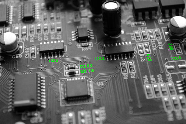
Advanced manufacturing systems will use artificial intelligence and machine learning algorithms to monitor copper plating conditions, predict process variations, and automatically optimize production parameters.
At the same time, higher-performance materials and advanced manufacturing techniques will allow PCBs to achieve improved thermal management and stronger current handling capabilities while maintaining compact designs.
Manufacturers that continuously improve their process control systems will be better positioned to provide reliable PCB solutions for next-generation electronic products.
PCB Copper Thickness Control is not a single manufacturing operation but a complete quality management process covering copper deposition, etching, surface treatment, and inspection.
Stable copper thickness directly influences electrical conductivity, thermal performance, and long-term reliability. Through optimized process control, accurate inspection methods, and continuous improvement systems, manufacturers can ensure that every PCB meets strict performance requirements.
As electronic devices become more powerful and compact, maintaining precise PCB Copper Layer Thickness will remain a critical factor in achieving excellent PCB Current Carrying Capacity.
By combining advanced manufacturing technologies with professional quality management, gopcba provides reliable PCB solutions that support customers in developing high-performance electronic products.