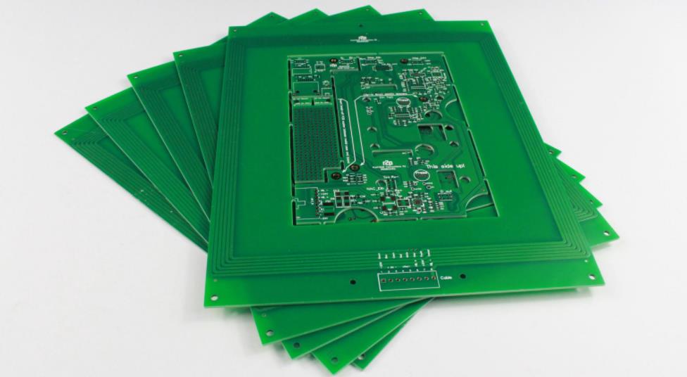
Design for Manufacturability (DFM) is a design methodology focused on making printed circuit boards easier, more reliable, and more cost-effective to manufacture. It is also a core technology of concurrent engineering, which brings design and manufacturing considerations together from the early stages of product development.
Design and manufacturing are two of the most critical stages in a product’s life cycle. In traditional development processes, designers may complete a PCB design first and only later discover that certain features are difficult or expensive to manufacture. PCB DFM addresses this problem by considering manufacturing requirements during the design stage.
Concurrent engineering requires designers to consider manufacturability, assembly, reliability, material selection, production processes, and cost from the beginning. Therefore, Design for Manufacturability has become an important tool for improving communication between PCB design and manufacturing teams.
The key purpose of DFM is to analyze whether design data can be processed by manufacturing equipment, evaluate manufacturing feasibility, identify potential production risks, and provide recommendations for improving the design.
This article summarizes the general PCB Design Guidelines and manufacturing requirements commonly considered during the DFM review of single-sided and double-sided PCBs.
1. General Requirements
As a general requirement for PCB Manufacturing, these guidelines establish a common reference between PCB design and fabrication. Their purpose is to improve communication between CAD and CAM data and reduce unnecessary design modifications during production.
1.1 CAD and CAM Communication
All design information required for PCB fabrication should be clearly defined in the design files. The manufacturing data should accurately describe:
- Board outline and dimensions
- Copper layers
- Trace width and spacing
- Pads and vias
- Plated and non-plated holes
- Solder mask openings
- Silkscreen information
- Slots and cutouts
- V-CUT requirements
- Surface finish requirements
- Special manufacturing instructions
Clear and consistent design data allows the manufacturing team to perform a more accurate DFM analysis.
1.2 Manufacturing Data Priority
When processing customer files, Kingda will primarily use the customer’s approved PCB drawings, Gerber files, drill files, and other manufacturing documentation as the basis for production.
If inconsistencies exist between different design documents, clarification should be obtained before manufacturing begins.
2. PCB Materials
2.1 PCB Substrate
For general-purpose single-sided and double-sided PCBs, the substrate is typically an FR-4 epoxy-glass laminate with copper foil.
FR-4 provides a good balance of:
- Mechanical strength
- Electrical insulation
- Thermal stability
- Processability
- Cost efficiency
Different laminate materials may be required for high-frequency, high-temperature, flexible, or other specialized applications.
2.2 Copper Foil
The copper foil used for standard PCBs is generally electrolytic copper with a purity of more than 99.9%.
For a standard double-sided PCB, the finished outer-layer copper thickness is typically approximately 35 μm (1 oz) unless otherwise specified.
If a different finished copper thickness is required, the requirement should be clearly indicated in the PCB drawing or manufacturing documentation.
3. PCB Structure, Dimensions, and Tolerances
3.1 PCB Structure
All relevant design elements that define the PCB structure should be clearly represented in the design files.
The PCB outline and mechanical features should preferably be defined on the Mechanical 1 layer or another clearly designated mechanical/keep-out layer according to the CAD system used.
When multiple mechanical layers are used, their functions should be clearly identified to prevent confusion during CAM processing.
For example:
- Board outlines should be clearly defined.
- Long slots should be represented using appropriate mechanical geometry.
- Cutouts should have complete and closed profiles.
- Internal openings should be clearly identified.
- Areas requiring special mechanical processing should be documented.
A clear mechanical definition helps prevent incorrect board profiling during fabrication.
3.2 Board Thickness Tolerance
The finished PCB thickness should meet the requirements specified in the design documentation.
When no specific tolerance is provided, the acceptable tolerance should be determined according to the board material, manufacturing process, and agreed manufacturing specification.
For precision applications, the required finished thickness and tolerance should always be specified on the fabrication drawing.
3.3 Board Outline Tolerance
The external dimensions of the PCB should comply with the dimensions specified in the design drawing.
If no dimensional tolerance is specified, a general tolerance of approximately ±0.20 mm may be applied for standard mechanically routed boards. Different tolerances may apply to V-CUT or other special manufacturing processes.
3.4 PCB Flatness and Warpage
PCB flatness should meet the requirements defined in the design documentation.
For boards used in SMT assembly, excessive warpage should be avoided because it can affect:
- Solder paste printing
- Component placement
- Reflow soldering
- BGA solder joints
- Board handling
- Automated assembly reliability
The acceptable warpage level should therefore be considered during both PCB design and manufacturing.
4. PCB Traces and Pads
4.1 PCB Layout Requirements
The PCB Layout, trace width, spacing, and pad dimensions should generally follow the approved PCB design.
However, manufacturing compensation may be required because copper etching, plating, and other fabrication processes can affect the final dimensions of traces and pads.
Kingda may apply appropriate process compensation according to manufacturing requirements while maintaining the electrical and functional intent of the original design.
When the designed trace spacing is below the recommended manufacturing capability, the design should be reviewed before production.
For standard single-sided and double-sided boards, Kingda generally recommends the following design values whenever the application allows:
- Minimum via finished hole diameter: 0.30 mm
- Recommended via pad diameter: 0.70 mm or larger
- Recommended minimum trace width: 8 mil
- Recommended minimum trace spacing: 8 mil
These values help reduce manufacturing difficulty and production cycle time.
For more advanced fabrication, Kingda may support smaller geometries depending on the PCB material, layer structure, copper thickness, aspect ratio, and manufacturing process.
For example, a minimum drill tool diameter may be approximately 0.30 mm, while a finished hole may be around 0.15 mm under specific fabrication conditions. Minimum trace width and spacing may reach approximately 6 mil, although such designs normally require tighter process control and may increase manufacturing cost and lead time.
Therefore, designers should avoid using the absolute manufacturing limit unless it is necessary for the application.
4.2 Trace Width Tolerance
The final trace width may vary slightly from the nominal design value because of etching and other fabrication processes.
As a general internal process reference, trace-width variation may be controlled within approximately ±15%, depending on copper thickness, line geometry, etching conditions, and board construction.
For critical impedance-controlled or high-speed circuits, the required trace width and impedance should be verified with the PCB manufacturer before production.
5. Copper Pour and Thermal Pad Design
5.1 Copper Grid Design
Large solid copper areas can experience thermal stress during processes such as wave soldering and PCB assembly.
For certain single-sided PCB applications, a copper grid pattern may be considered to reduce thermal stress and minimize the risk of:
- Copper lifting
- Board deformation
- Localized thermal stress
- Uneven soldering
Where a copper grid is required, a typical reference is:
- Grid spacing: ≥10 mil
- Grid line width: ≥10 mil
Depending on manufacturing capability, values should generally not be reduced below approximately 8 mil without prior DFM review.
However, solid copper planes may be preferable for applications requiring low impedance, high current capacity, or controlled return-current paths. Therefore, the choice between solid copper and grid copper should consider both electrical and manufacturing requirements.
5.2 Thermal Relief Pads
When component pads are connected directly to a large copper plane, heat can be transferred away from the pad too quickly during soldering.
This may make it difficult to achieve a reliable solder joint.
A thermal relief pattern can be used to connect the pad to the copper plane through several narrow copper spokes.
Thermal relief helps balance:
- Electrical conductivity
- Heat dissipation
- Solderability
- Manufacturing consistency
It is particularly useful for through-hole components connected to large ground or power areas.
6. Hole and Via Design
6.1 PTH and NPTH
PCB holes can generally be classified as:
- PTH (Plated Through Hole)
- NPTH (Non-Plated Through Hole)
PTH holes have conductive copper plating on their inner walls and are normally used for electrical interconnection or plated component holes.
NPTH holes do not have copper plating and are generally used for:
- Mechanical mounting
- Positioning
- Structural features
- Mechanical clearance
When the CAD design explicitly identifies a mounting hole as NPTH, Kingda will process it as a non-plated hole.
Mechanical layers may also be used to define mechanical holes or cutouts, provided the design documentation clearly identifies their intended function.
All other component holes, mounting holes, and through-holes that require electrical interconnection should be clearly defined as plated holes.
6.2 Hole Diameter and Tolerance
For component holes and mounting holes, the finished hole diameter should generally be specified in the PCB fabrication drawing.
A typical hole diameter tolerance may be approximately ±3 mil (0.08 mm), depending on the manufacturing process.
For via holes, the manufacturing tolerance may be controlled differently. As a general reference, a negative tolerance is normally avoided, while the positive tolerance may be controlled within approximately +3 mil (0.08 mm).
For critical holes, designers should always specify the required finished hole size and tolerance rather than relying on default values.
6.3 Plated Hole Copper Thickness
For plated through holes, the average copper thickness inside the hole wall is generally not less than approximately 20 μm, with the minimum local thickness typically controlled to approximately 18 μm or according to the applicable manufacturing specification.
Adequate hole-wall copper thickness is important for ensuring mechanical strength and long-term electrical reliability.
6.4 Hole Wall Roughness
The roughness of PTH hole walls should be controlled according to the manufacturing process and board requirements.
A typical reference value may be approximately 32 μm or less.
For high-reliability applications, hole-wall quality should be evaluated together with drilling parameters, desmear, copper plating, aspect ratio, and thermal cycling requirements.
7. PCB Tooling and PIN Hole Design
7.1 Tooling Holes
For CNC positioning, the minimum positioning pin diameter may be approximately 0.90 mm.
When three tooling holes are used for positioning, they should preferably be arranged in a triangular pattern to provide stable mechanical positioning.
7.2 Adding Tooling Holes
If the customer design does not include appropriate tooling holes and no special restrictions are specified, Kingda may recommend adding suitable tooling holes in an appropriate unused area of the PCB.
Tooling holes should be positioned so that they do not interfere with:
- Electrical circuits
- Copper planes
- Components
- Board outline
- SMT assembly
- Testing structures
Any such modification should be confirmed when it affects the customer’s functional or mechanical requirements.
8. Slot and Cutout Design
8.1 Slot Definition
The shape of a slot should preferably be defined on the Mechanical 1 layer or another clearly identified mechanical layer.
A slot may also be represented using a series of connected holes, but the hole dimensions should be consistent and the hole centers should be aligned correctly.
8.2 Minimum Slot Width
A typical minimum milling cutter diameter may be approximately 0.65 mm.
Therefore, designers should avoid excessively narrow slots unless the required manufacturing capability has been confirmed in advance.
8.3 Isolation Slots
For slots designed to provide electrical isolation between high-voltage and low-voltage regions, a wider slot may be preferable.
A slot diameter or width greater than approximately 1.20 mm can provide better manufacturability while also helping maintain the required electrical clearance.
The actual isolation distance should always be determined according to the applicable safety standard, working voltage, pollution degree, material characteristics, and end-use environment.
9. Solder Mask Design
9.1 Solder Mask Coverage
Except for areas such as solder pads, fiducial marks, test points, and other intentionally exposed copper, PCB surfaces should generally be covered with solder mask.
The solder mask defines the areas where copper remains exposed for soldering or electrical contact.
When copper areas are intentionally exposed for soldering or thermal purposes, the corresponding openings should be clearly defined in the solder mask layer.
9.2 Copper Features Defined by FILL or TRACK
If a customer uses FILL or TRACK objects to represent areas that require soldering or exposed copper, the corresponding solder mask opening should be clearly defined.
For improved design clarity and manufacturing consistency, Kingda recommends using dedicated pad or solder-mask definitions rather than relying solely on non-standard FILL or TRACK objects.
9.3 Solder Mask Adhesion
Solder mask adhesion should comply with the applicable PCB quality and acceptance requirements.
For general PCB production, solder mask quality should be evaluated for:
- Adhesion
- Coverage
- Color consistency
- Pinholes
- Bubbles
- Scratches
- Misregistration
- Cured condition
The final requirements should follow the agreed customer specification and applicable IPC standards.
9.4 Solder Mask Thickness
Solder mask thickness depends on the material, coating method, board surface, copper pattern, and manufacturing process.
For applications requiring controlled solder mask thickness, the required range should be specified in the fabrication documentation.
10. PCB Silkscreen and Etched Markings
10.1 Basic Silkscreen Requirements
PCB silkscreen should be designed for good readability while maintaining adequate clearance from pads and other conductive features.
A typical reference design is:
- Character height: 30 mil or larger
- Character stroke width: 5 mil or larger
- Character spacing: 4 mil or larger
These dimensions help prevent characters from becoming blurred or unreadable during PCB fabrication.
10.2 Etched or Copper Markings
Copper markings should not unintentionally connect to or bridge conductive traces.
Adequate electrical clearance must be maintained between copper markings and surrounding conductors.
A typical reference for etched characters is:
- Character height: 30 mil
- Character width: 7 mil or larger
For critical identification marks, designers should prioritize readability and electrical clearance rather than minimizing character size.
10.3 Automatic Silkscreen Adjustment
If the customer does not specify exact character dimensions, Kingda may make appropriate manufacturing adjustments to improve readability and prevent interference with pads, traces, and other PCB features.
10.4 Manufacturer Information
When no customer-specific restrictions apply, manufacturer identification, part numbers, production codes, or other required information may be placed on an appropriate silkscreen area.
Such markings should never interfere with component pads, fiducials, test points, or other functional features.
11. Silkscreen and SMT Pad Clearance
Silkscreen should not overlap solder pads because this can reduce solderability and potentially cause soldering defects.
When silkscreen overlaps an SMT pad, Kingda may adjust the silkscreen position or trim the affected section where appropriate.
The adjustment should preserve the intended relationship between the reference designator and the corresponding component.
Designers should maintain sufficient clearance between:
- Silkscreen and SMT pads
- Silkscreen and fiducials
- Silkscreen and exposed copper
- Silkscreen and board edges
This is especially important for densely populated PCBs.
12. Fiducial Mark Design
12.1 Fiducial Layer Concept
For double-sided boards, the top layer is generally treated as the primary component side unless otherwise specified.
The corresponding silkscreen and component identification information should be correctly oriented for manufacturing and assembly.
For single-sided boards, the signal layer should be clearly defined so that the intended viewing and component side can be correctly interpreted during CAM processing.
12.2 SMT Fiducials
When a PCB panel contains SMT components and automated placement equipment requires fiducial marks for positioning, appropriate fiducials should be included.
A typical global fiducial may use a circular exposed copper area with a diameter of approximately 1.0 mm.
Fiducials should have sufficient clearance from surrounding copper, solder mask openings, silkscreen, and other features.
12.3 Solder Mask Opening Around Fiducials
When no special requirement is specified, a solder mask opening of approximately 1.5 mm around the fiducial may be used as a general reference to improve machine recognition.
The corresponding opening should be defined on the appropriate solder mask layer, such as F.Mask.
12.4 Panel Fiducials
When a PCB panel contains SMT components and has a process edge, fiducial marks should normally be positioned on the process edge in suitable locations.
If a panel contains SMT components but does not include a process edge, the fiducial requirements should be reviewed based on the assembly equipment and customer requirements.
Proper fiducial placement helps SMT equipment accurately recognize PCB position and improve component placement accuracy.
13. V-CUT Design Guidelines
13.1 V-CUT Clearance
There is normally no gap between adjacent boards in a V-CUT panel.
However, sufficient clearance must be maintained between the V-CUT centerline and copper traces or other conductive features.
As a general reference, the distance between conductive features and the V-CUT line should be greater than approximately 0.5 mm on both sides.
This means that conductive features should generally be kept at least approximately 0.25 mm away from the intended board edge on each side, depending on the actual manufacturing process.
13.2 V-CUT Definition
The V-CUT line should be clearly defined in the mechanical design data.
The required V-CUT location can be represented using the appropriate mechanical layer, such as Mechanical 1, with clear markings or fabrication notes identifying the intended V-CUT position.
The mechanical data should clearly distinguish V-CUT lines from routed board outlines.
13.3 Remaining Thickness
After V-CUT processing, the remaining material thickness is typically around one-third of the original PCB thickness, although the actual remaining thickness can be adjusted according to customer requirements and board construction.
The correct V-CUT depth should balance:
- Panel strength during assembly
- Ease of depanelization
- Edge quality
- Component stress
- Board thickness
13.4 V-CUT Edge Quality
After depanelization, the glass-fiber structure near the V-CUT edge may become slightly loose or extend beyond the nominal board dimensions.
In some cases, the edge variation may exceed approximately 0.5 mm, depending on laminate construction and depanelization conditions.
Therefore, V-CUT should not be used where curved outlines or complex shapes are required.
13.5 V-CUT Shape Restrictions
A V-CUT tool normally travels in a straight line.
Therefore, V-CUT cannot normally be used to create:
- Curved outlines
- Irregular contours
- Bent cutting paths
- Non-linear profiles
For irregular board shapes, CNC routing or a combination of routing and V-CUT should be considered.
As a general reference, V-CUT is more commonly applied to boards with a thickness of approximately 0.8 mm or greater, although the actual capability depends on the PCB construction and equipment.
14. PCB Surface Finish
When no special surface-finish requirement is specified, the surface finish should be selected according to the application and manufacturing agreement.
Traditional HAL (Hot Air Leveling) is one commonly used PCB surface finish. Leaded HASL uses a tin-lead alloy, historically around 63% tin / 37% lead.
However, for modern electronic products, lead-free manufacturing requirements may require lead-free HASL, ENIG, OSP, immersion tin, immersion silver, or another surface finish.
The surface finish should therefore be selected according to:
- Product application
- Soldering process
- Environmental requirements
- RoHS compliance
- Shelf life
- Fine-pitch component requirements
- Cost
- Reliability requirements
For fine-pitch components and high-density PCB designs, ENIG or other advanced surface finishes may provide advantages over conventional HASL.
15. Why DFM Matters in PCB Manufacturing
A successful PCB Manufacturing process begins with a design that takes manufacturing limitations into account.
A PCB design may be electrically correct but still create manufacturing problems if it includes:
- Extremely narrow traces
- Insufficient spacing
- Very small holes
- Inadequate annular rings
- Poor solder mask clearance
- Incorrect fiducial placement
- Inappropriate V-CUT locations
- Narrow slots
- Silkscreen overlapping pads
- Unclear mechanical data
- Excessively tight dimensional tolerances
These problems can lead to increased scrap rates, longer manufacturing cycles, additional engineering work, higher costs, and reduced product reliability.
A DFM review identifies these risks before fabrication begins.
16. Recommended PCB DFM Design Checklist
Before releasing PCB files for manufacturing, designers should verify the following:
Electrical Design
- Trace width meets manufacturing requirements.
- Trace spacing provides sufficient electrical clearance.
- High-current traces have adequate copper width.
- Controlled-impedance requirements are clearly specified.
- Ground and power structures are correctly defined.
Hole and Via Design
- Hole sizes are compatible with the selected manufacturing process.
- PTH and NPTH holes are clearly identified.
- Via dimensions meet aspect-ratio requirements.
- Annular rings are sufficiently large.
- Mechanical holes are clearly defined.
Mechanical Design
- Board dimensions are clearly specified.
- Board outline is closed and unambiguous.
- Slots and cutouts are correctly defined.
- V-CUT locations are clearly marked.
- Copper is kept away from board edges where required.
Solder Mask and Silkscreen
- Solder mask openings are correctly defined.
- Silkscreen does not overlap solder pads.
- Character sizes are large enough to remain readable.
- Reference designators are correctly positioned.
- Fiducial marks have sufficient clearance.
Manufacturing Documentation
- Gerber files are complete.
- Drill files are complete.
- Mechanical drawings are consistent with fabrication data.
- Layer names and functions are clearly identified.
- Copper thickness is specified.
- Board thickness is specified.
- Surface finish is specified.
- Special manufacturing requirements are documented.
17. Conclusion
The above PCB Design Guidelines provide a general reference for single-sided and double-sided PCB design and manufacturing. They are intended to improve communication between CAD design data and CAM manufacturing processes while reducing avoidable production risks.
The goal of Design for Manufacturability is not simply to make a PCB design easier to fabricate. More importantly, DFM establishes a common understanding between designers and manufacturers before production begins.
By considering trace width, spacing, holes, vias, solder mask, silkscreen, fiducials, board dimensions, V-CUT, surface finish, and other manufacturing factors during the design stage, engineers can significantly reduce manufacturing problems.
For complex or high-density PCB projects, early communication with Kingda can help designers determine appropriate manufacturing capabilities and optimize the design before production.
Ultimately, effective PCB DFM helps shorten the product development and manufacturing cycle, reduce production costs, improve yield, and enhance the overall reliability of the finished PCB.