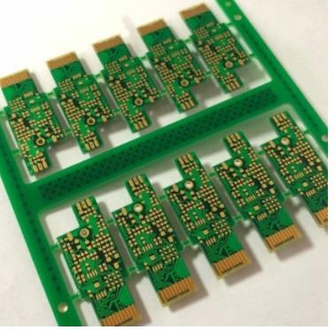
In Multilayer PCB manufacturing, PCB Pre-Baking is an important process performed after liquid photoresist coating and before exposure and development. Its primary purpose is to remove excess moisture and solvents from the photoresist surface, creating a stable film condition for subsequent photolithography.
Proper pre-baking directly affects the adhesion, exposure quality, development performance, and dimensional accuracy of the circuit pattern. If the process is not properly controlled, problems such as poor exposure, film adhesion to the phototool, incomplete development, and pattern defects may occur.
The most commonly used equipment for the Pre-Baking Process includes tunnel ovens and temperature-controlled drying ovens. The pre-baking operation is generally performed in or near the coating area to minimize contamination and unnecessary handling.
What Is PCB Pre-Baking?
After a liquid photoresist is applied to the PCB surface, the coating still contains solvents and moisture. Before the board enters the exposure process, the film must reach an appropriate dry condition.
PCB Pre-Baking uses controlled heating to partially remove these volatile components and stabilize the photoresist film.
The objective is not simply to make the film completely dry. Instead, the process must achieve the specific film condition required by the photoresist manufacturer’s specifications.
A properly controlled PCB Pre-Baking process should provide:
- Uniform photoresist drying
- Stable film adhesion
- Appropriate residual solvent content
- Good exposure characteristics
- Consistent development performance
- Improved pattern definition
- Reduced risk of photoresist defects
Common PCB Pre-Baking Equipment
Two common methods are used in PCB Manufacturing: tunnel ovens and conventional drying ovens.
Tunnel Oven
A tunnel oven continuously transports PCB panels through a controlled heating zone. Temperature, airflow, conveyor speed, and residence time can be controlled to achieve consistent drying.
Tunnel ovens are particularly suitable for high-volume production because they provide relatively stable and repeatable process conditions.
Temperature-Controlled Drying Oven
A conventional oven can also be used for PCB Pre-Baking, provided that it has adequate temperature control and air circulation.
The oven should preferably be equipped with:
- Forced-air circulation
- Uniform temperature distribution
- Accurate temperature control
- Clean internal surfaces
- Appropriate ventilation
- Reliable temperature monitoring
Uniform airflow is particularly important because temperature differences inside the oven can cause inconsistent photoresist drying across the PCB panel.
Cleanliness Is Essential
The drying chamber must be kept clean and free of dust, particles, oil, and other contaminants.
Because the liquid photoresist forms the surface layer used for image transfer, contamination introduced during pre-baking can become a permanent defect in the subsequent Exposure and Development process.
Particles may result in:
- Pinholes
- Open circuits
- Incomplete imaging
- Local photoresist adhesion problems
- Pattern contamination
- Defective circuit features
Therefore, regular cleaning and preventive maintenance of the oven are essential parts of Process Control.
Why Natural Drying Is Not Recommended
Natural drying generally does not provide the consistency required for modern Multilayer PCB production.
Ambient temperature, humidity, airflow, and drying time can vary significantly. As a result, the photoresist may not reach a stable and repeatable condition before exposure.
Insufficient drying can leave excessive moisture or solvent in the film. This may make the surface more sensitive to pressure and increase the risk of the photoresist sticking to the phototool during exposure.
On the other hand, excessive drying can make the photoresist more difficult to develop or strip.
Controlled thermal processing is therefore preferred because it provides a more predictable film condition.
Cooling Before Exposure
After PCB Pre-Baking is completed, the PCB panel should be cooled appropriately before exposure.
Depending on the process specification, the panel may be allowed to cool under controlled conditions or use forced-air cooling.
The key objective is to ensure that the photoresist reaches the required processing temperature before the exposure operation begins.
Exposing the board while it is still excessively hot can affect photoresist behavior and may introduce variation in the exposure process.
For this reason, cooling conditions should also be included in the overall Process Control strategy.
Time Between Coating, Pre-Baking, and Development
After photoresist coating and pre-baking, the PCB should proceed through exposure and development within the time window specified by the photoresist manufacturer.
Long storage periods can expose the coated panel to changes in temperature and humidity, potentially affecting the photoresist condition.
Humidity deserves particular attention. In high-humidity environments, moisture absorption can influence photoresist performance and increase the risk of exposure or development defects.
Therefore, production scheduling should minimize unnecessary waiting time between:
Photoresist Coating → PCB Pre-Baking → Cooling → Exposure → Development
For sensitive materials, the manufacturer’s technical data sheet should be used to establish the maximum allowable hold time.
Different Photoresists Require Different Parameters
There is no single pre-baking temperature and time that is suitable for every Liquid Photoresist.
Different photoresist formulations may have different requirements for:
- Coating thickness
- Baking temperature
- Baking time
- Airflow
- Exposure energy
- Cooling time
- Development conditions
- Stripping conditions
For this reason, production engineers should always refer to the technical data provided by the Liquid Photoresist manufacturer.
The actual parameters should then be validated against the production line, equipment characteristics, PCB material, panel size, and coating thickness.
The Importance of Temperature Control
Temperature is one of the most critical parameters in the Pre-Baking Process.
If the temperature is too high, or the baking time is excessive, the photoresist may become over-baked. This can change its chemical properties and make subsequent development or stripping more difficult.
Potential consequences include:
- Slow development
- Incomplete film removal
- Residual photoresist
- Poor pattern definition
- Increased process variation
Conversely, insufficient temperature or baking time may leave the film inadequately dried.
This can result in:
- Photoresist tackiness
- Phototool adhesion
- Exposure defects
- Surface damage
- Uneven development
The process window must therefore be optimized rather than simply maximizing the drying temperature.
The Relationship Between Photoresist Thickness and Baking
Photoresist thickness also influences the required PCB Pre-Baking conditions.
A thicker photoresist layer generally contains more solvent and requires sufficient time for uniform drying throughout the film.
However, simply increasing temperature or baking time is not always the correct solution.
Excessive thermal exposure can alter the photoresist properties near the surface while the internal portion of the film may behave differently.
Production engineers should therefore evaluate the combination of:
Photoresist Thickness + Temperature + Time + Airflow
rather than controlling each parameter independently.
Humidity Control During Photoresist Processing
Environmental conditions can have a significant influence on Multilayer PCB photolithography.
High humidity may increase moisture absorption, while excessively dry conditions may affect handling and static-related contamination.
The coating, pre-baking, exposure, and development areas should therefore be maintained within the environmental range recommended for the specific photoresist system.
Stable environmental conditions help reduce variation between production batches.
How PCB Pre-Baking Affects Exposure
The quality of Exposure and Development depends heavily on the condition of the photoresist film.
A properly pre-baked film should provide a stable surface that can accurately receive the image from the phototool.
If the film remains too wet or tacky, it may adhere to the phototool and damage the image transfer process.
If the film is over-baked, its photosensitive properties may change, potentially affecting exposure sensitivity and development behavior.
Therefore, PCB Pre-Baking should be considered an integral part of the photolithography process rather than an isolated drying step.
How PCB Pre-Baking Affects Development
After exposure, the PCB enters the development stage, where unwanted portions of the photoresist are removed.
The development rate is closely related to the photoresist’s chemical condition.
Improper pre-baking may cause:
- Excessively slow development
- Incomplete development
- Residual photoresist
- Uneven pattern edges
- Difficulty removing unexposed film
- Variation in line width
Properly controlled baking helps produce a photoresist condition that develops consistently and provides better circuit-pattern definition.
Process Monitoring and Verification
A stable Pre-Baking Process requires more than setting a nominal oven temperature.
Kingda recommends monitoring process conditions through a combination of equipment verification, temperature measurement, material control, and production inspection.
Important control points include:
- Verify oven temperature uniformity.
- Monitor actual board temperature rather than relying only on the oven set point.
- Control baking time consistently.
- Confirm photoresist coating thickness.
- Monitor environmental temperature and humidity.
- Keep the oven clean.
- Control the waiting time before exposure.
- Inspect exposure and development results.
- Record process parameters for traceability.
Periodic temperature mapping can also help identify hot or cold zones within the oven.
Common PCB Pre-Baking Problems
Several problems can be traced back to inappropriate pre-baking conditions.
Under-Baking
When the photoresist is insufficiently dried, the film may remain tacky or contain excessive residual solvent.
This increases the risk of phototool adhesion and exposure defects.
Over-Baking
Excessive temperature or baking time may make the photoresist difficult to develop or strip and can reduce process stability.
Uneven Baking
If airflow or temperature distribution is inconsistent, different areas of the PCB panel may have different photoresist conditions.
This can lead to variations in line width and development behavior.
Contamination
Dust or particles inside the oven can settle on the coated PCB surface and create localized defects.
Excessive Waiting Time
Long delays between coating, baking, exposure, and development can expose the photoresist to environmental changes and increase process variation.
Best Practices for PCB Pre-Baking
For reliable PCB Manufacturing, the following practices are recommended:
- Follow the photoresist manufacturer’s process specifications.
- Validate actual panel temperature rather than relying solely on oven settings.
- Maintain uniform airflow and temperature.
- Keep baking equipment clean.
- Control coating thickness.
- Maintain stable temperature and humidity.
- Allow sufficient cooling before exposure.
- Minimize storage time after coating and pre-baking.
- Monitor development performance.
- Establish process windows through production validation.
- Maintain complete process records.
Kingda’s Approach to PCB Pre-Baking
At Kingda, PCB Pre-Baking is treated as an important part of the overall photolithography process.
Process engineers consider photoresist characteristics, coating thickness, PCB structure, panel dimensions, oven performance, temperature distribution, environmental conditions, and downstream exposure and development requirements.
By controlling these parameters together, Kingda aims to maintain stable photoresist performance and consistent circuit-pattern quality across production batches.
Conclusion
PCB Pre-Baking is a critical step in Multilayer PCB manufacturing because it determines the condition of the photoresist before exposure and development.
The most important factors include baking temperature, baking time, airflow, photoresist thickness, environmental humidity, cooling, and the time between processing stages.
Under-baking can leave the photoresist tacky and increase the risk of exposure defects, while over-baking can make development and stripping more difficult. Uneven temperature distribution or contamination can also reduce pattern quality.
By establishing a controlled Pre-Baking Process, monitoring actual process conditions, and following the requirements of the selected Liquid Photoresist, manufacturers can achieve more consistent exposure, development, and circuit-pattern quality in PCB Manufacturing.