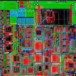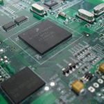
Multilayer PCB technology is widely used in high-speed and high-performance electronic systems because it provides greater routing density, better power distribution, and improved electromagnetic performance.
As electronic products become smaller and faster, PCB designers must carefully control signal return paths, impedance, crosstalk, power integrity, and electromagnetic compatibility. A well-designed multilayer board is not simply a PCB with more copper layers. Its layer stackup, reference planes, routing strategy, and via structures must work together to provide predictable electrical performance.
In most high-speed multilayer boards, some layers are dedicated to power or ground reference planes. These planes are typically designed as large, continuous copper areas whenever possible. Regardless of whether a plane is used for power distribution or grounding, it can also influence the return-current path of adjacent signal layers.
Therefore, one of the most important objectives of multilayer PCB Design is to establish a low-impedance and continuous return-current path.
Multilayer PCB Stackup Structure
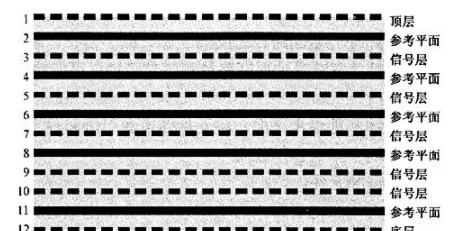
A typical multilayer PCB Stackup consists of signal layers positioned between solid reference planes.
Signal layers are often placed between power and ground planes to form symmetrical or asymmetrical stripline structures. The close relationship between signal traces and reference planes helps control characteristic impedance and confines electromagnetic fields.
The top and bottom layers are generally used for component placement, solder pads, and short signal connections. Although these outer layers can also contain signal traces, critical high-speed traces should not be unnecessarily long because exposed traces can increase electromagnetic radiation and coupling.
Common layer notation includes:
- P — Power or reference plane
- S — Signal layer
- T — Top layer
- B — Bottom layer
A practical multilayer stackup may therefore contain alternating signal and reference-plane layers, depending on the number of layers, routing density, impedance requirements, and power-distribution architecture.
The exact stackup should be determined according to the electrical and mechanical requirements of the product rather than simply following a fixed layer arrangement.
1. Define Reference-Plane Voltages and Power Distribution
One of the most important aspects of multilayer PCB Design is establishing a stable reference-plane structure.
Decoupling capacitors are essential for maintaining local power integrity and suppressing high-frequency power noise. Their effectiveness depends heavily on placement and connection geometry.
A decoupling capacitor should be positioned as close as possible to the IC power pins. The connection between the capacitor, power plane, and ground plane should be short and wide, with an appropriate via structure.
For example, a multilayer PCB may use one inner layer as a power plane for high-speed digital devices such as processors and another inner layer as a solid ground plane. Decoupling capacitors can then be placed on the top layer near the processor, with short connections to the power and ground structures.
This arrangement can reduce parasitic inductance and provide a lower-impedance high-frequency current path.
When planning the stackup, designers should also consider the reference plane used by critical high-speed signals. Whenever possible, signals generated by the same high-speed device should have consistent and continuous reference structures.
2. Carefully Plan Split Power Planes
Modern systems often require multiple supply voltages. A single power layer may therefore be divided into several physical regions to distribute different voltage domains.
However, split power planes can create problems for high-speed signal return currents.
If a high-speed signal is routed over a gap or split in its reference plane, its return current may be forced to travel around the discontinuity. This increases the effective current-loop area and can cause impedance discontinuities, additional radiation, crosstalk, and Signal Integrity problems.
For this reason, critical high-speed signals should generally avoid crossing gaps in power or reference planes.
Ground planes are often preferable as high-speed signal references because they can provide a more continuous return path than heavily segmented power planes.
If a signal must transition between different reference regions, the return-current path should be carefully evaluated and, where appropriate, supported with a suitable stitching or coupling structure.
3. Use Multiple Ground Planes
Multiple ground planes can significantly improve the electrical performance of a multilayer PCB.
A continuous ground plane provides a low-impedance return path and can reduce the loop area of high-frequency currents. It can also help reduce common-mode electromagnetic radiation and improve EMC performance.
Ground planes are particularly useful for high-speed digital, RF, and mixed-signal circuits because they provide a stable reference for controlled-impedance transmission lines.
However, simply adding more ground layers does not automatically guarantee better performance. The ground planes must be connected properly, and their relationship with signal layers, power planes, and vias must be considered during the stackup design.
4. Closely Couple Signal Layers to Reference Planes
A signal layer should be closely coupled to its adjacent reference plane.
In practical PCB Stackup design, this means keeping the dielectric thickness between the signal layer and its reference plane sufficiently small and well controlled.
A smaller dielectric spacing generally reduces the electromagnetic field area around the trace and can make impedance control more predictable. It also helps reduce the susceptibility of the signal to external electromagnetic interference.
The relationship between trace width, copper thickness, dielectric thickness, and dielectric constant determines the characteristic impedance of a transmission line.
Therefore, impedance-controlled routing should be designed together with the actual PCB material and stackup rather than treating trace width as an independent parameter.
Power and ground planes should also be positioned appropriately to reduce power-distribution impedance and improve high-frequency current return.
5. Properly Plan Signal Routing Layer Pairs
Complex multilayer boards inevitably require signals to transition between routing layers.
The selection of routing layer combinations is important because every layer transition can affect the signal’s return-current path.
When a signal changes from one routing layer to another, the return current must also transition between the corresponding reference structures. If the reference planes are not properly aligned, the return current may be forced to travel through an unnecessarily long or discontinuous path.
For example, if signal layer 3 references ground layer 4 and signal layer 5 references ground layer 6, these layers can form a practical routing combination when the transition between them is properly designed.
In contrast, using widely separated signal layers that require the return current to cross multiple reference structures can create a less desirable return path.
A poorly designed transition can increase loop inductance, ground bounce, electromagnetic radiation, and signal distortion.
When a signal changes layers, designers should therefore evaluate:
- The reference plane associated with each signal layer
- The distance between the signal and reference plane
- The location of nearby ground vias
- Whether the reference plane is continuous
- Whether the return current has a low-impedance transition path
- Whether the via structure introduces excessive parasitic inductance
For critical high-speed signals, via transitions should be designed as part of the complete transmission-line structure.
6. Establish a Consistent Routing Direction
Routing direction should be planned systematically across different signal layers.
A common approach is to route the majority of traces on one signal layer in one primary direction and use an approximately perpendicular direction on the adjacent signal layer.
For example:
- Layer 3: primarily north-south routing
- Layer 5: primarily east-west routing
- Layer 7: primarily north-south routing
- Layer 9: primarily east-west routing
This strategy can reduce unnecessary parallel coupling between adjacent signal layers and make routing more organized.
However, routing direction should not be considered an absolute rule. Actual routing should also account for component placement, differential-pair requirements, critical signal paths, impedance control, and the available reference planes.
7. Control Return-Current Paths
A major principle of high-speed PCB Design is that every signal needs an appropriate return-current path.
At high frequencies, return current tends to follow the path of lowest impedance rather than simply taking the shortest physical route.
When a signal trace runs above a continuous reference plane, the return current is concentrated primarily in the reference plane directly beneath the signal. This creates a relatively small current loop and helps reduce electromagnetic radiation.
If the reference plane is interrupted by a split, void, or large clearance, the return current must travel around the discontinuity. The resulting larger loop can increase inductive coupling and EMI.
Therefore, designers should avoid unnecessary gaps beneath critical high-speed signal traces.
8. Optimize Via and Layer Transitions
Vias are essential in high-density multilayer boards, but excessive use of vias can degrade high-speed electrical performance.
Each via introduces parasitic inductance and capacitance. At high frequencies, these parasitic effects can become significant and create impedance discontinuities.
For critical signals, designers should minimize unnecessary layer transitions and consider:
- Via diameter
- Via pad size
- Anti-pad dimensions
- Via stub length
- Back-drilling requirements
- Ground-via placement
- Signal-via spacing
- Differential-pair symmetry
Ground vias should be positioned appropriately around high-speed and RF structures to provide a low-inductance return path between reference planes.
9. Consider Signal Integrity During Stackup Design
Signal Integrity should be considered from the beginning of the multilayer PCB development process.
Important parameters include:
- Characteristic impedance
- Trace width and spacing
- Dielectric thickness
- Dielectric constant
- Copper thickness
- Copper roughness
- Signal rise/fall time
- Via parasitics
- Return-current paths
- Crosstalk
- Plane discontinuities
A stackup that looks acceptable from a routing-density perspective may still produce poor electrical performance if the signal-to-plane relationship is not properly controlled.
For this reason, stackup design, material selection, impedance calculation, and routing rules should be developed as an integrated process.
10. Design Power and Ground Structures Together
Power integrity and signal integrity are closely related in modern multilayer PCBs.
A rapidly switching digital device can generate transient currents that cause voltage fluctuations across the power-distribution network. If the power and ground structures have excessive impedance, these fluctuations can propagate through the board and interfere with sensitive circuits.
A well-designed Power Plane can provide a low-impedance distribution network, while a solid ground plane provides a stable return path.
Decoupling capacitors should be distributed according to the current requirements and frequency characteristics of the devices. High-frequency decoupling should be placed close to the IC power pins, while bulk capacitance can be positioned according to the broader power-distribution architecture.
11. Apply Design Rules According to Manufacturing Capability
Electrical performance is only one part of successful PCB Manufacturing.
The stackup and routing strategy must also comply with the manufacturer’s actual fabrication capabilities. Important manufacturing parameters include:
- Minimum trace width
- Minimum trace spacing
- Minimum via diameter
- Copper thickness
- Layer registration accuracy
- Dielectric thickness tolerance
- Impedance tolerance
- Aspect ratio
- Surface finish
- Board thickness
Design rules that exceed the manufacturer’s process capability may increase fabrication cost, reduce yield, or create reliability problems.
Therefore, designers should communicate with the PCB manufacturer before finalizing complex multilayer structures.
Kingda Multilayer PCB Manufacturing Support
Kingda provides PCB manufacturing solutions for applications requiring high-density routing, multilayer structures, controlled impedance, and reliable electrical performance.
For complex multilayer projects, Kingda can support key manufacturing requirements such as multilayer fabrication, fine-line routing, controlled impedance, via structures, copper-thickness control, registration accuracy, and customized stackup requirements.
A successful multilayer PCB requires close coordination between design and manufacturing. The stackup should be reviewed not only for routing capacity but also for signal integrity, power integrity, thermal performance, manufacturability, and long-term reliability.
By considering these factors early in the design process, engineers can reduce unnecessary redesigns and improve the consistency of the final PCB.
Conclusion
The core principle of multilayer PCB Design is to establish a predictable relationship between signal layers, reference planes, power distribution, and return-current paths.
A well-designed PCB Stackup should provide:
- Continuous and low-impedance reference planes
- Controlled signal-to-plane coupling
- Appropriate power-plane distribution
- Short and predictable return-current paths
- Proper routing-layer combinations
- Controlled impedance
- Minimized via discontinuities
- Effective grounding and decoupling
- Adequate manufacturing margins
As electronic systems continue to become faster and more compact, multilayer PCB design must move beyond simple routing-density considerations. Careful stackup planning, power and ground management, routing-direction control, and Signal Integrity analysis are essential for achieving stable high-speed performance.
Working with an experienced PCB Manufacturing partner such as Kingda can further help ensure that complex multilayer designs are translated into manufacturable, reliable, and consistent physical boards.